Charge Separation Part 1: Diode Lecture 5 9/22/2011 MIT - PowerPoint PPT Presentation
Charge Separation Part 1: Diode Lecture 5 9/22/2011 MIT Fundamentals of Photovoltaics 2.626/2.627 Fall 2011 Prof. Tonio Buonassisi 1 2.626/2.627 Roadmap You Are Here Buonassisi (MIT) 2011 2 2.626/2.627: Fundamentals Every
Charge Separation Part 1: Diode Lecture 5 – 9/22/2011 MIT Fundamentals of Photovoltaics 2.626/2.627 – Fall 2011 Prof. Tonio Buonassisi 1
2.626/2.627 Roadmap You Are Here Buonassisi (MIT) 2011 2
2.626/2.627: Fundamentals Every photovoltaic device must obey: Output Energy Conversion Efficiency Input Energy For most solar cells, this breaks down into: Inputs Outputs Charge Light Charge Charge Charge Solar Spectrum Drift/Diff Absorption Excitation Separation Collection usion total absorption excitation drift/diffusion separation collection Buonassisi (MIT) 2011 3
Liebig’s Law of the Minimum S. Glunz, Advances in Optoelectronics 97370 (2007) total absorption excitation drift/diffusion separation collection Image by S. W. Glunz. License: CC-BY. Source: "High-Efficiency Crystalline Silicon Solar Cells." Advances in OptoElectronics (2007). Buonassisi (MIT) 2011 4
Diode: Essence of Charge Separation • What is a diode? N P • How is it made? • Why care about diodes? I N P I Buonassisi (MIT) 2011 5
Diode: Essence of Charge Separation Courtesy of Adrio Communications Ltd. Used with permission. http://www.radio-electronics.com/info/data/thermionic- valves/vacuum-tube-theory/tube-tutorial-basics.php Buonassisi (MIT) 2011 6
Learning Objectives: Diode 1. Describe how conductivity of a semiconductor can be modified by the intentional introduction of dopants. 2. Draw pictorially, with fixed and mobile charges, how built- in field of pn-junction is formed. 3. Current flow in a pn -junction: Describe the nature of drift, diffusion, and illumination currents in a diode. Show their direction and magnitude in the dark and under illumination. 4. Voltage across a pn -junction: Quantify the built-in voltage across a pn -junction. Quantify how the voltage across a pn - junction changes when an external bias voltage is applied. 5. Draw current-voltage (I-V) response, recognizing that minority carrier flux regulates current. Buonassisi (MIT) 2011 7
Dopant Atoms Periodic Table http://pvcdrom.pveducation.org/ Courtesy of PVCDROM. Used with permission. Buonassisi (MIT) 2011 8
Carrier Binding Energy to Shallow Dopant Atoms Carrier binding energy to a shallow (hydrogenic) dopant atom: m * 1 m * 1 E E H 2 13.6 eV 2 m e m e Courtesy of PVCDROM. Used with permission. Buonassisi (MIT) 2011 9
Carrier Binding Energy to Shallow Dopant Atoms Effective mass Carrier binding energy to a shallow correction (hydrogenic) dopant atom: m * 1 m * 1 E E H 2 13.6 eV 2 m e m e Courtesy of PVCDROM. Used with permission. Electron screening Buonassisi (MIT) 2011 10
Learning Objectives: Diode 1. Describe how conductivity of a semiconductor can be modified by the intentional introduction of dopants. 2. Draw pictorially, with fixed and mobile charges, how built-in field of pn-junction is formed. 3. Current flow in a pn -junction: Describe the nature of drift, diffusion, and illumination currents in a diode. Show their direction and magnitude in the dark and under illumination. 4. Voltage across a pn -junction: Quantify the built-in voltage across a pn -junction. Quantify how the voltage across a pn - junction changes when an external bias voltage is applied. 5. Draw current-voltage (I-V) response, recognizing that minority carrier flux regulates current. Buonassisi (MIT) 2011 11
Gauss’ Law: Review Spatially variant fixed charge creates an electric field: d dx = electric field = charge density = material permittivity Example: Capacitor Capacitor Image by MIT OpenCourseWare. Buonassisi (MIT) 2011 12
Gauss’ Law: Review Spatially variant fixed charge creates an electric field: d dx = electric field = charge density = material permittivity Drift Current: Net charge moves parallel to electric field Described by Drift Equation J h q h p J e q e n From: PVCDROM Courtesy of PVCDROM. Used with permission. Buonassisi (MIT) 2011 13
Diffusion: Review Described by Fick’s Law dp J h qD h dx dn J e qD e dx From PVCDROM Courtesy of PVCDROM. Used with permission. Buonassisi (MIT) 2011 14
Recall the Checker Board Example Si Si Si Si Si Si Si Si Si Si Si Si Si Si Si Si + - Si Si Si Si Si Si Si Si Si Si Si Si Si Si Si Si Buonassisi (MIT) 2011 15
Let’s imagine the n - and p-type materials in contact, but with an imaginary barrier in between them. Buonassisi (MIT) 2011 16
How a pn-junction comes into being Courtesy of PVCDROM. Used with permission. Buonassisi (MIT) 2011 17
When that imaginary boundary is removed, electrons and holes diffuse into the other side. Buonassisi (MIT) 2011 18
How a pn-junction comes into being Courtesy of PVCDROM. Used with permission. Eventually, the accumulation of like charges [(h + + P + ) or (e - + B - )] balances out the diffusion, and steady state condition is reached. Buonassisi (MIT) 2011 19
How a pn-junction comes into being Courtesy of PVCDROM. Used with permission. Solid line = Approximate charge distr. Net Charge Dashed line = Real charge distribution Position The net charge can be approximated as shown above. Buonassisi (MIT) 2011 20
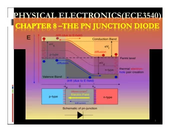
How a pn-junction comes into being qN D Courtesy of PVCDROM. Used with permission. Net Charge Position qN A Electric Field d dx Position Potential d o V A dx Position e - Energy E q q o V A Position Buonassisi (MIT) 2011 21
Summary of Current Understanding Courtesy of PVCDROM. Used with permission. e - Energy E q q o V A Position 1. When light creates an electron-hole pair, a pn - junction can separate the positive and negative charges because of the built-in electric field. 2. This built-in electric field is established at a pn- junction because of the balance of electron & hole drift and diffusion currents. Buonassisi (MIT) 2011 22
In-Class Exercise Buonassisi (MIT) 2011 23
2.626/2.627 Lecture 5 (9/22/2011) pn -junction, under dark conditions No Bias Forward Bias Reverse Bias Model - + Circuit P N P N P N - + - + E E E p-type n-type p-type n-type p-type n-type Band Diagram x x x e - diffusion: e - diffusion: e - diffusion: e - drift: e - drift: e - drift: I I I I-V Curve V V V Buonassisi (MIT) 2011 24
2.626/2.627 Lecture 5 (9/22/2011) pn -junction, under dark conditions No Bias Forward Bias Reverse Bias Model - + Circuit P N P N P N - + - + E E E p-type n-type p-type n-type p-type n-type Tasks: 1. Draw band diagram (electron energy as a Band function of position). Diagram 2. Draw relative magnitudes of electron drift x x x and diffusion currents. e - diffusion: e - diffusion: e - diffusion: e - drift: e - drift: e - drift: I I I I-V Curve V V V Buonassisi (MIT) 2011 25
2.626/2.627 Lecture 5 (9/22/2011) pn -junction, under dark conditions No Bias Forward Bias Reverse Bias Model - + Circuit P N P N P N - + - + E E E p-type n-type p-type n-type p-type n-type Band Diagram x x x e - diffusion: e - diffusion: e - diffusion: e - drift: e - drift: e - drift: I I I I-V Curve V V V Buonassisi (MIT) 2011 26
2.626/2.627 Lecture 5 (9/22/2011) pn -junction, under dark conditions No Bias Forward Bias Reverse Bias Model - + Circuit P N P N P N - + - + E E E p-type n-type p-type n-type p-type n-type Band Diagram x x x h + diffusion: e - diffusion: e - diffusion: h + drift: e - drift: e - drift: I I I I-V Curve V V V Buonassisi (MIT) 2011 27
2.626/2.627 Lecture 5 (9/22/2011) pn -junction, under dark conditions No Bias Forward Bias Reverse Bias Model - + Circuit P N P N P N - + - + E E E p-type n-type p-type n-type p-type n-type Tasks: 1. Represent a voltage bias source ( e.g. , battery) Band on the model circuit diagram. Ensure that Diagram positive and negative terminals of the battery x x x are pointing in the correct directions. e - diffusion: e - diffusion: e - diffusion: e - drift: e - drift: e - drift: I I I I-V Curve V V V Buonassisi (MIT) 2011 28
2.626/2.627 Lecture 5 (9/22/2011) pn -junction, under dark conditions No Bias Forward Bias Reverse Bias + - - + Model - + Circuit P N P N P N - + - + E E E p-type n-type p-type n-type p-type n-type Band Diagram x x x e - diffusion: e - diffusion: e - diffusion: e - drift: e - drift: e - drift: I I I I-V Curve V V V Buonassisi (MIT) 2011 29
2.626/2.627 Lecture 5 (9/22/2011) pn -junction, under dark conditions No Bias Forward Bias Reverse Bias + - - + Tasks: 1. Draw energy band diagrams, under forward Model and reverse bias (in the dark). - + Circuit 2. Draw relative magnitudes of electron drift P N P N P N - + - + and diffusion currents. E E E p-type n-type p-type n-type p-type n-type Band Diagram x x x e - diffusion: e - diffusion: e - diffusion: e - drift: e - drift: e - drift: I I I I-V Curve V V V Buonassisi (MIT) 2011 30
Recommend
More recommend
Explore More Topics
Stay informed with curated content and fresh updates.


![1 Prof. S. Ben-Yaakov , DC-DC Converters [5- 4] Average power = + I I I cos( t](https://c.sambuz.com/1027954/1-s.webp)
