Carbon Nanotubes for Transistor Type-Biosensor and Therapeutic - PowerPoint PPT Presentation
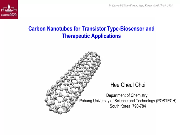
5 th Korea-US NanoForum, Jeju, Korea, April 17-18, 2008 Carbon Nanotubes for Transistor Type-Biosensor and Therapeutic Applications Hee Cheul Choi Department of Chemistry, Pohang University of Science and Technology (POSTECH) South Korea,
5 th Korea-US NanoForum, Jeju, Korea, April 17-18, 2008 Carbon Nanotubes for Transistor Type-Biosensor and Therapeutic Applications Hee Cheul Choi Department of Chemistry, Pohang University of Science and Technology (POSTECH) South Korea, 790-784
Surface Chemistry of Carbon nanotubes: Hybrid structures Facile and spontaneous synthetic approaches Choi, et al., JACS 2002 , 124, 9059. Noble metal-SWNT composites Lee and Choi, et al., Small 2005 , 1, 975. Transition metal-SWNT TiO 2 -SWNT composites Mechanism Shin and Choi, et al., Adv. Mater . 2007 , 19 , 2873.
Surface Chemistry of Carbon nanotubes: Schottky diodes Intercalation of Li ions in pyrene-functionalized SWNT Schottky diode behavior Lithium intensity distribution (SPEM, Li 1s) Modulation of band energy Lim and Choi, et al., JACS 2008 , 130, 2160.
Surface Chemistry of Carbon nanotubes: Carbothermal Reduction – Etching SiO 2 CO CH 4 H 2 SiO C 2 H 4 O 2 SiO 2 Si Carbothermal Reduction Byon and Choi, Nature Nanotech 2007 , 2, 162. Byon and Choi, Nano Lett. 2008 , 8, 178.
Sub-10 nm scale Lithography using Nanotrenches Byon and Choi, Nature Nanotech 2007 , 2, 162.
Carbon nanotube electronics: Carbon nanotube/protein-based memory device Negative Differential Resistance (NDR) device - Ferritin captured in metallic SWNT nanogap electrodes - Electrically cut m-SWNT (gap = ca. 20 nm) - Electrostatically captured Ferritins - Peak current density: 4.0 x 10 6 A cm -2 (record) - Peak-to-Valley Ratio (PVR): ~ 40 (@ scan rate of 26 mV/s) - NDR is 1.2 µ ohm cm 2 Apoferrtin + Fe(III) Apoferrtin Tang and Choi, et al., JACS 2007 , 129, 11018.
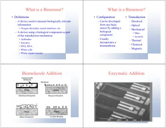
Electronic sensing of biomolecular recognitions using SWNTs-FETs ▪ Nonspecific Binding ▪ Specific Binding ( using CDI-Tween20 ) Robert J. Chen et al ,. PNAS . 2003 , 100 , 4984
Hurdles to overcome Sensitivity - At least ~ pM, grateful if it can go lower. - Protein detection limit of SWNT-FET: >10 nM (c.f. Lieber group: ~ 10 fM detection limit of proteins using SiNW devices- Nat. Biotechol . 2005 , 23 , 1294 .) Feasibility - Prompt use: currently too long stabilization time - Nonspecific binding: perfect protection of devices with efficient chemical blocking is mandatory.
The two regions effecting to a biosensor sensitivity Buffer Sol’n Au/Cr Au/Cr SiO 2 /Si Nanotube aspect: Direct charge communication between proteins and nanotubes Metal-nanotube contact aspect: Schottky barrier modulation by protein adsorptions on metal surfaces
The origin of conductance changes: Schottky Barrier � Nanotube aspects: Charge injection from biomolecules Electric double layer field modulation caused by biomolecules Strongly depending on the pI (isoelectric point) values of proteins � Metal-nanotube contact aspect: Adsorbed chemical species may modulate work function level of contact metals , which consequently change the Schottky barrier height resulting in the conductance change. Energy CB E FM + E FS buffer VB Fermi level matching (E FM = E FS ) & Semiconducting Metal Band bending of VB, SWNT CB
Experimental evidence for the detection mechanism PMMA HIgG SWNT -6 .50x10 SiO 2 /Si 1.48 Pd/Au I ds ( µΑ) evaporation Device I 100 nM 1.46 SiO 2 /Si mPEG-SH s SAM 1.44 0 400 800 1200 Time (s) Lift off s s sssssssss s -6 .50x10 SiO 2 /Si 100 nM 3.45 Lift off I ds ( µΑ) Device II 3.40 ss s s 3.35 SiO 2 /Si SiO 2 /Si 3.30 OMe OMe 0 200 400 600 800 1000 O O Time (s) n n S S Device II Device I Chen, Choi, Dai et al, J. Am. Chem. Soc . 2004 , 126 , 1563
Increased Schottky contact area for high performance Au/Cr Au/Cr SiO 2 /Si ▪ Synthesis of network SWNTs ▪ Usage of the thin shadow mask ▪ Thermal evaporator with tilted angle stages
Fabrication of SWNT-FET having increased Schottky contact area SiO 2 /Si Substrate with Catalyst D S SiO 2 /Si CH 4 ( R ~ 1 k Ω ) H 2 C 2 H 4 S D CVD (900 ℃ 10 min) (Cu) Growth SWNTs In wire Teflon Protein Injection electrochemical cell 2000 μ m 10 mV V S D 1 μ M 200 µ m Choi and Dai et al. Nano Lett . 2003 , 3, 157. Yang and Choi et al . Langmuir 2005 , 21, 9198.
Fabrication of SWNT-FET having increased Schottky contact area (a) SWNT FET device fabricated by a photolithography Au/Cr Photo Resist SWNTs SiO 2 /Si (2) Lift Off (1) Metal Evaporation Au/Cr Shadow Mask SWNTs SiO 2 /Si angle evaporation (b) SWNT-FET device fabricated by a shadow mask at tilted angle Byon and Choi. J. Am. Chem. Soc . 2006 , 128, 2188.
Highly sensitive SWNT-FET devices: Nonspecific bindings of proteins Buffer sol’n A u / C r S i O 2 / S i a SWNT-FET fabricated by a shadow mask ▪ SA at tilted angle ▪ SpA � 1 pM sensitivity Byon and Choi. J. Am. Chem. Soc . 2006 , 128, 2188.
Highly sensitive SWNT-FET devices: Nonspecific bindings of proteins (unit : pM) a SWNT-FET fabricated by a shadow mask a SWNT-FET fabricated by a shadow mask at tilted angle <Protein : SpA> � 1 pM sensitivity � 10 nM sensitivity
Highly sensitive SWNT-FET devices: Specific bindings of proteins ▪ Probe protein: Protein A ▪ Probe protein: hCG ▪ Target protein: anti β -hCG ▪ Target protein: rabbit IgG Treatment of 0.05% Tween20 after immobilizing probe proteins � 1 pM sensitivity
Acknowledgement Post Doctors Dr. Hyeon Suk Shin Dr. Hye Ryung Byon Graduate Students Seok Min Yoon Yoonmi Lee Hyun Jae Song Hyunseob Lim Hye Kyung Moon Suphil Kim Kyoung Ok Kim Ji Eun Park Kwangho Chu UnderGraduate Students Chee Bum Park January 8, 2008 Collaborators Prof. Joon Won Park (POSTECH) Prof. Jillian M. Buriak (Univ. Alberta, Canada) Prof. Insung S. Choi (KAIST) Fundings Prof. Seunghun Hong (SNU) MOST, KOSEF, KRF, POSTECH Prof. Jin Yong Lee (SKKU) Prof. Young Kyun Kwon (U. Mass)
Recommend
More recommend
Explore More Topics
Stay informed with curated content and fresh updates.



![Transistor Channel Model [Farquhar and Hasler, 2004] Transistor HH Channel Model [Farquhar and](https://c.sambuz.com/897541/transistor-channel-model-s.webp)
