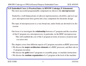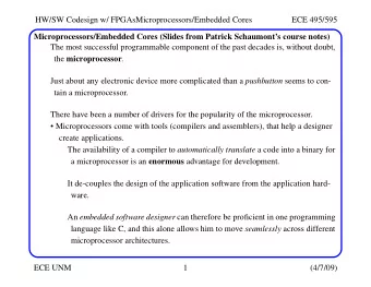
Built-In Self-Test for Regular Structure Embedded Cores in - PowerPoint PPT Presentation
Built-In Self-Test for Regular Structure Embedded Cores in System-on-Chip Srinivas Murthy Garimella Masters Thesis Defense Thesis Advisor : Dr. Charles E. Stroud Committee Members : Dr. Victor P. Nelson & Dr. Adit D. Singh Department of
Built-In Self-Test for Regular Structure Embedded Cores in System-on-Chip Srinivas Murthy Garimella Master’s Thesis Defense Thesis Advisor : Dr. Charles E. Stroud Committee Members : Dr. Victor P. Nelson & Dr. Adit D. Singh Department of ECE, Auburn University The VLSI Design & Test Seminar Series March 23, 2005
Outline � Motivation � Background � RAM BIST for Atmel SoCs � SoC Architecture � VHDL approach � AVR approach � RAM BIST for Xilinx FPGAs � FPGA Architecture � VHDL approach � Conclusions and Future Research The VLSI Design & Test Seminar Series March 23, 2005 2
Motivation � Testing of VLSI Chips � Up to 50-60% of manufacturing cost � System-on-Chip (SoC) � $43.2 billion industry by 2009 (BCC) � Embedded memory � Currently about 50% of SoC die area � Can grow up to 90% by 2010 (ITRS 2004) The VLSI Design & Test Seminar Series March 23, 2005 3
Motivation (Contd..) � Embedded memory cores � Increase density � Increase die size � Decrease yield � Testing Embedded memory cores � Critical in SoCs The VLSI Design & Test Seminar Series March 23, 2005 4
Background � System-on-Chip (SoC) � Integration of various components (IP cores like processor, memory, FPGA) onto a single silicon chip � Elimination of interconnect effect on device performance � Realization due to advancement in semiconductor processing techniques � Communication products currently form its largest market segment The VLSI Design & Test Seminar Series March 23, 2005 5
Configurable SoCs (CSoCs) � SoCs with embedded Field Programmable Gate Array (FPGA) � Fixing design errors and reduce re-spin costs � Reusability for implementing different functions � Implementing DSP algorithms � Remote upgrades The VLSI Design & Test Seminar Series March 23, 2005 6
Field Programmable Gate Arrays (FPGAs) � Programmable Elements Interconnect Network � Logic Blocks (PLBs) � Interconnect network � Input Output Buffers PLB PLB PLB (IOBs) � Embedded memory components PLB PLB PLB � Coarse grained – dedicated memories � requires memory/ logic partitioning during FPGA design PLB PLB PLB � Fine grained – distributed memories � avoids poor memory utilization IOB The VLSI Design & Test Seminar Series March 23, 2005 7
RAM Functional Model Vdd 1 2 5 6 Word 3 4 Word Bit Bit 6-Transistor SRAM Cell � RAM Types – SRAM, DRAM, Flash, etc., � Ports – Single-port, Dual-port, Multi-port � Modes - Synchronous, Asynchronous � Sizes – Different data widths and address widths The VLSI Design & Test Seminar Series March 23, 2005 8
Memory Testing � Functional testing � No knowledge of memory circuit implementation required � Fully functional test – 2 n complexity where n = number of cells in the array � Subset of likely to occur faults – Fault model The VLSI Design & Test Seminar Series March 23, 2005 9
Fault Models � Address decoder and Data line faults � Refresh Logic and Sense Amplifier faults 0 1 1 0 � Cell-related faults � Stuck-At faults � Transition faults � Coupling faults (CFs) � Aggressor and Victim cells � Inter-word and Intra-word CFs n n n � Neighborhood pattern sensitive faults (NPSFs) - base cell and neighboring n b n cells n n n � Static –base cell forced to a certain value � Passive – base cell changes � Active – base cell cannot change � Multi-port memory faults The VLSI Design & Test Seminar Series March 23, 2005 10
Memory Test Algorithms � Traditional tests � Checkerboard, Walking 1/ 0, Butterfly � Order of complexity: n 2 , n× log 2 n � Not sufficient for detecting all faults � March Tests � Order of complexity: n � Different march tests for different fault models � Sequence of reads and writes The VLSI Design & Test Seminar Series March 23, 2005 11
March Tests � Notation � ↓ : addressing downward ↑ : addressing upward ↨ : either way Algorithm Notation w0: write 0 ↨ (w0); ↓ (r0, w1); r1: read 1 March � ↑ (r1,w0,r0,r0, w1); Length = 16 N , N = number of memory LR w/ o cells ↑ (r1,w0); BDS � ↑ (r0,w1,r1,r1,w0); ↑ (r0); Wider-Memories � Background Data Sequences (BDS) ↨ (w00); ↓ (r00, w11); March � Detects intra-word CFs ↑ (r11,w00,r00,r00, w11); LR with � Detects Bridging faults ↑ (r11,w00); BDS � Detects NPSFs ↑ (r00,w11,r11,r11,w00); � Number of BDS = log 2 ( K )+ 1, where ↑ (r00,w01,w10,r10); K = data width ↑ (r10,w01,r01); � For e.g., BDS for 4-bit wide memory : 0000(1111),0101(1010),0011(1100) ↑ (r01); The VLSI Design & Test Seminar Series March 23, 2005 12
AT94K SoC Architecture Config Config � Three IP Cores FPGA FPGA memory memory � FPGA � Up to 48x48 array of PLBs � Embedded Free RAMs Data Data � SRAM RAM RAM � Dual-port Data SRAM � Single-port Program SRAM Program Program Memory Memory � 8-bit RISC Processor RISC RISC � Can write into FPGA Processor Processor configuration memory � Dynamic Partial Reconfiguration Peripherals Peripherals The VLSI Design & Test Seminar Series March 23, 2005 13
FPGA Architecture � Arranged in 4x4 array of PLBs � PLB � Two 3-input LUTs � D Flip-Flop FPGA Core Array FPGA Core Array � Multiplexers PLB PLB PLB PLB PLB PLB � Local routing to adjacent Y Y X X X X PLBs PLB PLB PLB PLB PLB PLB Y Y Y Y X X X X Y Y � 4 Directs (Y) PLB PLB PLB PLB PLB PLB � 4 Diagonals (X) PLB local routing PLB local routing The VLSI Design & Test Seminar Series March 23, 2005 14
FPGA Architecture (cont… ) � Global routing- 5 planes Vertical Routing Planes Vertical Routing Planes Horizontal Routing Horizontal Routing � Two x8 lines per plane � Two x4 lines per plane Planes Planes � Repeaters provide buffering and connection � Free RAMs PLB PLB � One 32x4 RAM for every PLB global routing PLB global routing 4x4 array of PLBs 4 � Single-port or dual-port Din 5 operation Wadd 5 32x4 32x4 � Synchronous or Radd WE RAM RAM Asynchronous operation OE Dout 4 The VLSI Design & Test Seminar Series March 23, 2005 15
Free RAM Routing The VLSI Design & Test Seminar Series March 23, 2005 16
Free RAM Testing � Three modes of testing � Single-port synchronous � Single-port asynchronous � Dual-port synchronous � Asynchronous read � Not a true dual-port � Test approach � Built-In Self-Test (BIST) � Advantages: � Minimal use of testers � At-speed testing � No X-states problem with memories � No fault-coverage problem as BIST relies on march tests for fault coverage � Disadvantages: � Area overhead (not for FPGAs) � Lower performance The VLSI Design & Test Seminar Series March 23, 2005 17
BIST Approach � Logic BIST approach � TPG TPG TPG TPG TPG TPG TPG � Single � Dual RUT BUT BUT RUT BUT RUT BUT RUT BUT RUT BUT RUT BUT RUT BUT RUT � ORA � Expected Data ORA ORA ORA ORA ORA ORA ORA ORA comparison � Adjacent RAM BUT RUT RUT BUT BUT RUT RUT BUT BUT BUT RUT BUT RUT BUT RUT RUT Comparison � Number of test configurations The VLSI Design & Test Seminar Series March 23, 2005 18
BIST Implementation (Dual-port testing) Dual-Port RAM test ORA design � TPG – assuming logic and routing to be fault free � March DPR test algorithm (w/ o BDS) - ↨ (w0 : n); ↓ (n : r0); ↑ (w1 : ↓ r1); ↓ (w0 : ↑ r0); � VHDL Implementation – 66 PLBs � ORA � Comparison with data from adjacent RAM � Lack of enough routing resources prevented implementation of expected data comparison The VLSI Design & Test Seminar Series March 23, 2005 19
BIST Implementation (Single-port testing) Single-Port RAM test ORA Design � TPG � March LR with BDS in synchronous mode � VHDL Implementation – 123 PLBs � March Y w/ o BDS in asynchronous mode ↨ (w0); ↑ (r0; w1; r1); ↓ (r1; w0; r0); ↑ (r0); � VHDL Implementation – 18 PLBs � ORA � Comparison with expected data generated by TPG The VLSI Design & Test Seminar Series March 23, 2005 20
Implementation Issues � VHDL approach � No control over placement with Atmel’s tool – makes diagnosis difficult � Solutions: � Manual placement – tedious � Maintain mapping information – may change with synthesis � Irregular routing � Problems fitting BIST circuitry in smaller devices � Alternate approach � Macro Generation language (MGL) � Similar to VHDL � Atmel proprietary HDL � Control over placement and routing � PLBs are primitive logic elements The VLSI Design & Test Seminar Series March 23, 2005 21
Implementation Issues (cont… ) Shift In � Define relative placement of Y RAMs and ORAs � Define interconnection between X X RAMs and ORAs Y X X � TPG implementation in MGL not simpler Y � VHDL-MGL mixed approach � Best solution X X � Implement TPG in VHDL Y X X � Implement rest of the BIST circuitry in MGL Dout Dout Shift out � Helps in implementing processor RAM1 RAM2 BIST The VLSI Design & Test Seminar Series March 23, 2005 22
Routing Issues solved with MGL The VLSI Design & Test Seminar Series March 23, 2005 23
Recommend
More recommend
Explore More Topics
Stay informed with curated content and fresh updates.

