Advances in Averaged Switch Modeling and Simulation Dragan - PowerPoint PPT Presentation
1999 Power Electronics Specialists Conference Advances in Averaged Switch Modeling and Simulation Dragan Maksimovic * and Robert Erickson Colorado Power Electronics Center CoPEC http://ece-www.colorado.edu/~pwrelect * Acknowledgment: the work
A few points regarding averaged switch modeling • The switch network can be defined arbitrarily, as long as its terminal voltages and currents are independent, and the switch network contains no reactive elements. • It is not necessary that some of the switch network terminal quantities coincide with inductor currents or capacitor voltages of the converter, or be nonpulsating. • The object is simply to write the averaged equations of the switch network; i.e., to express the average values of half of the switch network terminal waveforms as functions of the average values of the remaining switch network terminal waveforms, and the control input.
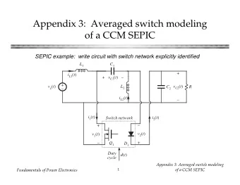
Terminal waveforms of the switch network v 1 ( t ) v C 1 + v C 2 L 1 C 1 v 1 ( t ) T s + i L 1 ( t ) + v C 1 ( t ) – 0 0 + 0 dT s T s t v g ( t ) L 2 v C 2 ( t ) C 2 R – i 1 ( t ) i L 1 + i L 2 i L 2 ( t ) – i 1 ( t ) T 2 i 1 ( t ) i 2 ( t ) Switch network 0 0 – + 0 dT s T s t v 2 ( t ) v 1 ( t ) v 2 ( t ) v C 1 + v C 2 + – Q 1 D 1 v 2 ( t ) T 2 Duty d ( t ) cycle 0 0 0 dT s T s t i 2 ( t ) i L 1 + i L 2 i 2 ( t ) T s 0 0 0 dT s T s t
t + Ts The averaging step T s = 1 x ( t ) x ( t ) dt T s t Now average all waveforms over one switching period: Power input Load Averaged time-invariant network + containing converter reactive elements 〈 v g (t) 〉 T s + C 〈 v(t) 〉 T s L R – 〈 i L (t) 〉 T s + 〈 v C (t) 〉 T s – – 〈 i 1 (t) 〉 T s 〈 i 2 (t) 〉 T s + + Averaged port 1 port 2 switch network 〈 v 1 (t) 〉 T s 〈 v 2 (t) 〉 T s – – Control d(t) input
The averaging step The basic assumption is made that the natural time constants of the converter are much longer than the switching period, so that the converter contains low-pass filtering of the switching harmonics: One may average the waveforms over an interval that is short compared to the system natural time constants, without significantly altering the system response. In particular, averaging over the switching period T s removes the switching harmonics, while preserving the low-frequency components of the waveforms. This step removes the small but mathematically-complicated switching harmonics, leading to a relatively simple and tractable converter model. In practice, the only work needed for this step is to average the switch dependent waveforms.
Averaged terminal equations of the switch network (small switching ripple is neglected) v 2 ( t ) v 1 ( t ) v C 1 + v C 2 v C 1 + v C 2 v 1 ( t ) T s v 2 ( t ) T 2 0 0 0 0 0 dT s T s 0 dT s T s t t v 1 ( t ) T s = d '( t ) v C 1 ( t ) T s + v C 2 ( t ) v 2 ( t ) T s = d ( t ) v C 1 ( t ) T s + v C 2 ( t ) T s T s i 2 ( t ) i 1 ( t ) i L 1 + i L 2 i L 1 + i L 2 i 2 ( t ) T s i 1 ( t ) T 2 0 0 0 0 0 dT s T s t 0 dT s T s t i 1 ( t ) T s = d ( t ) i L 1 ( t ) T s + i L 2 ( t ) i 2 ( t ) T s = d '( t ) i L 1 ( t ) T s + i L 2 ( t ) T s T s
Derivation of switch network equations (Algebra steps) We can write Result i 1 ( t ) T s i L 1 ( t ) T s + i L 2 ( t ) T s = d ( t ) + 〈 i 1 ( t ) 〉 T s – v 2 ( t ) d '( t ) d '( t ) + 〈 v 1 ( t ) 〉 T s 〈 v 2 ( t ) 〉 T s T s v 2 ( t ) T s i 1 ( t ) T s v C 1 ( t ) T s + v C 2 ( t ) T s = d ( t ) d ( t ) – d ( t ) 〈 i 2 ( t ) 〉 T s – + Hence Averaged switch network T s = d '( t ) v 1 ( t ) v 2 ( t ) d ( t ) T s Modeling the switch network via averaged dependent sources T s = d '( t ) i 2 ( t ) i 1 ( t ) d ( t ) T s
Steady-state switch model: Dc transformer model Original switch network i 1 ( t ) i 2 ( t ) Switch network – + v 2 ( t ) v 1 ( t ) + – Q 1 D 1 Duty d ( t ) cycle Averaged steady-state model: “DC transformer” I 1 D' : D + – • Correctly represents the relationships between the dc and low-frequency V 1 V 2 components of the terminal waveforms of the switch I 2 – + network
Steady-state CCM SEPIC model Replace switch network with dc transformer model L 1 C 1 + I L 1 + V C 1 – + L 2 V C 2 V g C 2 R – I L 2 – • Can now let inductors become short circuits, I 1 D' : D capacitors become open + – circuits, and solve for dc V 1 V 2 conditions. I 2 – + • Can simulate this model using PSPICE, to find transient waveforms
Modeling converter dynamics: Small-signal linearization of model d ( t ) = D + d ( t ) Perturb and linearize the switch network averaged waveforms v 1 ( t ) T s = V 1 + v 1 ( t ) about a quiescent operating i 1 ( t ) T s = I 1 + i 1 ( t ) point. Let: v 2 ( t ) T s = V 2 + v 2 ( t ) i 2 ( t ) T s = I 2 + i 2 ( t ) Voltage equation becomes D + d V 1 + v 1 = D ' – d V 2 + v 2 D V 2 + v 2 – d V 1 + V 2 V 1 + v 1 = D ' Eliminate nonlinear terms D and solve for v 1 terms: V 1 = D ' D V 2 + v 2 – d DD '
Linearization, continued Current equation becomes D + d I 2 + i 2 = D ' – d I 1 + i 1 Eliminate nonlinear terms and solve for i 2 terms: D I 1 + i 1 – d I 1 + I 2 I 2 + i 2 = D ' D I 2 = D ' D I 1 + i 1 – d DD '
Switch network: Small-signal ac model Reconstruct an equivalent circuit that corresponds to these small- signal equations: I 1 + i 1 D' : D + – – + V 1 DD ' d I 2 V 1 + v 1 V 2 + v 2 DD ' d + – I 2 + i 2 Transistor port Diode port A general small-signal ac model for the PWM switch network operating in CCM.
Small-signal ac model of the CCM SEPIC Replace switch network with small-signal ac model: L 1 C 1 + I L 1 + i L 1 V C 1 + v C 1 + L 2 C 2 V C 2 + v C 2 V g + v g R – I L 2 + i L 2 – D' : D + – Can now solve this V 1 model to determine ac DD ' d I 2 transfer functions DD ' d
Small-signal models of several basic switch networks I 1 + i 1 I 2 + i 2 i 1 (t) i 2 (t) 1 : D + – + + + + V 1 d V 1 + v 1 v 1 (t) V 2 + v 2 v 2 (t) I 2 d – – – – I 1 + i 1 I 2 + i 2 i 1 (t) i 2 (t) D' : 1 – + + + + + V 2 d V 1 + v 1 v 1 (t) v 2 (t) V 2 + v 2 I 1 d – – – – I 1 + i 1 I 2 + i 2 i 1 (t) D' : D i 2 (t) + – + + + + V 1 DD ' d I 2 V 1 + v 1 v 1 (t) V 2 + v 2 v 2 (t) DD ' d – – – –
Table of results Transfer functions of the basic buck, boost, and buck-boost converters Control-to-output and line-to-output transfer functions G vd ( s ) and G vg ( s ) ω 0 ω z G g0 G d0 Converter Q V 1 C R ∞ buck D D LC L 1 V D ' D ' 2 R C D ' R boost D ' D ' LC L L D ' 2 R – D V D ' C D ' R buck-boost D ' D D ' 2 LC L D L where the transfer functions are written in the standard forms 1 – s ω z 1 G vg ( s ) = G g 0 G vd ( s ) = G d 0 s s 2 1 + Q ω 0 + s ω 0 s 2 1 + Q ω 0 + ω 0
���������������������������� ��������������������������������� ccm1 � i 1 ( t ) i 2 ( t ) i 1 i 2 averaged-switch switch 1 3 + 1 3 model + + + network averaging D D (sub-circuit) K K 1-d v 1 ( t ) 1-d + i 1 v 2 ( t ) v 1 v 2 E t G d v 2 d – d S A S A _ _ _ _ 2 4 2 4 5 duty d • Controlled voltage source E t replaces the transistor, controlled current source G d replaces the diode • Duty ratio d is input to the subcircuit • Large-signal, nonlinear model suitable for DC, AC or Transient simulation • The same model can be applied in any two-switch PWM converter (the transistor and the diode need not have a common node) • Limitations: ideal switches, CCM only, valid for two-switch converters without isolation transformer
CCM Averaged-Switch Model PSpice Implementation: ccm1 ********************************************************** * MODEL: ccm1 averaged-switch D 1 3 K * Application: two-switch PWM converters network (sub-circuit) * Limitations: ideal switches, CCM only, no transformer + E t G d – ********************************************************** * Parameters: none S 2 4 A 5 ********************************************************** duty * Nodes: * 1: transistor+ (D) * 2: transistor- (S) * 3: diode cathode (K) U1 * 4: diode anode (A) D 4 A * 5: duty ratio (duty) 1 ccm1 ********************************************************** .subckt ccm1 1 2 3 4 5 2 3 K 5 S Et 1 2 value={(1-v(5))*v(3,4)/v(5)} duty Gd 4 3 value={(1-v(5))*i(Et)/v(5)} .ends **********************************************************
Sepic converter example using ccm1 model V L1 R1 C1 3 2x 2 4 1 800u 0.5 100u R2 0.1 Vg + C2 L2 R3 50V 100u - 100u 50 U1 D 4 A 1 ccm1 2 3 K 5 S duty + ACMAG=1V Vd sepic-ccm1.sch DC=0.5V - Objective: generate small-signal control-to-output frequency responses
������������������������������ ccm1 ������� ��������������������������������������� (A) sepic-ccm1.dat 80 magnitude || vout/d || 40 0 -20 DB(V(4)) 0d phase of vout/d -100d -200d small-signal control-to-output response Vout=50V, R=50, D=0.5 -270d 10Hz 100Hz 1.0KHz 10KHz 100KHz P(V(4)) Frequency
�������� • Subcircuit ccm1 is implementation of a large-signal, nonlinear averaged model of the switch network • Averaged circuit model of the converter is obtained simply by replacing switching devices with the averaged-switch subcircuit model • Linearization and AC small-signal analysis are performed by the simulator • Small-signal dynamic responses can be easily generated for different operating points or different sets of parameter values
������������������������� ������������������������������� • MOS transistor model: on-resistance R ON • Diode model: constant forward voltage drop V D in series with R d resistance i 1 ( t ) i 2 ( t ) • Switch network switch 1 3 + + network D K v 1 ( t ) v 2 ( t ) S A _ _ 2 4 v 1 ( t ) i 1 ( t ) v+V D +R d i i • Waveforms R on i t t 0 dT s T s 0 dT s T s v 2 ( t ) i 2 ( t ) v-R on i i t t -V D -R d i 0 dT s T s 0 dT s T s
�������������������������� ccm2 ������������������������������� v 1 ( t ) i 1 ( t ) = i d i v+V D +R d i i 1 T T s s = − R on i i ( 1 d ) i 2 T T s s t t 0 dT s T s 0 dT s T s 1 − v 2 ( t ) i 2 ( t ) d = v-R on i i i i 2 1 T T d s s t t -V D -R d i 0 dT s T s ) ( ) 0 dT s T s ( = + − + + 1 v dR i d v V R i 1 on D d T T T s s s + = v v v 1 2 T T T s s s ( ) ( ) − R i 1 d R i − 1 d on 1 d 1 = + + + T T v v V s s 1 1 D 2 T T d d d s s
CCM Averaged-Switch Model PSpice Implementation: ccm2 ********************************************************** * MODEL: ccm2 averaged-switch * Application: two-switch PWM converters, includes D 1 3 K sub-circuit + * conduction losses due to Ron, VD, Rd E ron – G d * Limitations: CCM only, no transformer + E t – ********************************************************** S 2 4 A 5 * Parameters: duty * Ron=transistor on resistance * VD=diode forward voltage drop (constant) Subcircuit implementation * Rd=diode on resistance ********************************************************** U2 * Nodes: (same as in ccm1) D 4 A ********************************************************** 1 .subckt ccm2 1 2 3 4 5 ccm2 +params: Ron=0 VD=0 Rd=0 2 3 K 5 S Eron 1 1x value={i(Et)*(Ron+(1-v(5))*Rd/v(5))/v(5)} duty Et 1x 2 value={(1-v(5))*(v(3,4)+VD)/v(5)} Gd 4 3 value={(1-v(5))*i(Et)/v(5)} .ends **********************************************************
Sepic converter example using ccm2 model V L1 R1 C1 3 2x 2 4 1 800u 0.5 100u R2 0.1 Vg + Iload C2 + 1A L2 50V 100u - - 100u 10K R4 U1 D 4 A 1 ccm2 2 3 K 5 S Ron={Ron} Rd=0.05 PARAMETERS: duty VD=0.8V 0.0 Ron + DC=0.5V Vd - Objective: find converter efficiency as a function of the transistor on-resistance, for a range of loads
������������������������������ ccm2 ������� ����������������������������������� (D) sepic-ccm2.dat 100 Efficiency [%] (only conduction losses are included) 95 R on =0 90 0.1 0.2 0.3 85 0.4 -100*V(4)* I(Iload)/ V(1)/ I(Vg) R on =0.5 80 1.0A 1.5A 2.0A 2.5A 3.0A 3.5A 4.0A 4.5A 5.0A I_Iload
�������������������������� ccm3 ����������������������������������������� Switch network Waveforms 1:n v 1 ( t ) i 1 ( t ) i v i 1 ( t ) i 2 ( t ) switch 1 3 + + network t t 0 dT s T s 0 dT s T s D K v 2 ( t ) i 2 ( t ) v 1 ( t ) v 2 ( t ) i/n S n v A _ _ 2 4 t t 0 dT s T s 0 dT s T s SECONDARY PRIMARY 1 − 1 − d d = = v v i i 1 2 2 1 T T T T nd nd s s s s • Converters: Flyback, Cuk, Sepic, Inverse Sepic (Zeta), with isolation transformer
CCM Averaged-Switch Model PSpice Implementation: ccm3 ********************************************************** * MODEL: ccm3 averaged-switch D 1 3 K network * Application: two-switch PWM converters, (sub-circuit) + * with (possibly) transformer E t G d – * Limitations: ideal switches, CCM only S 2 4 A ********************************************************** 5 duty * Parameters: * n=transformer turns ratio 1:n (primary:secondary) ********************************************************** * Nodes: (same as in ccm1) U3 ********************************************************** D 4 A .subckt ccm3 1 2 3 4 5 1 ccm3 +params: n=1 Et 1 2 value={(1-v(5))*v(3,4)/v(5)/n} 2 3 K 5 S Gd 4 3 value={(1-v(5))*i(Et)/v(5)/n} duty .ends **********************************************************
�������������������������� ccm4 ��������������������������������������������� • Combined ccm2 and ccm3 averaged-switch models • Parameters: • Transistor on resistance R on • Diode forward voltage drop V D • Diode on resistance R d • Transformer turns ratio n • A general model implementation valid for all two-switch converters operating in CCM
CCM Averaged-Switch Model PSpice Implementation: ccm4 * MODEL: ccm4 * Application: two-switch PWM converters, includes averaged-switch * conduction losses due to Ron, VD, Rd D 1 3 K sub-circuit + E ron * and (possibly) transformer – G d * Limitations: CCM only + E t – ********************************************************** S 2 4 A 5 * Parameters: duty * Ron=transistor on resistance * VD=diode forward voltage drop (constant) * Rd=diode on resistance Subcircuit implementation * n=transformer turns ratio 1:n (primary:secondary) ********************************************************** U4 * Nodes: (same as in ccm1) D 4 A ********************************************************** 1 .subckt ccm4 1 2 3 4 5 ccm4 +params: Ron=0 VD=0 Rd=0 n=1 2 3 K 5 S Eron 1 1x value={i(Et)*(Ron+(1-v(5))*Rd/n/n/v(5))/v(5)} duty Et 1x 2 value={(1-v(5))*(v(3,4)+VD)/v(5)/n} Gd 4 3 value={(1-v(5))*i(Et)/v(5)/n} .ends
���������������������������������� ���������������������� • Use averaged-switch modeling approach to construct an averaged model that includes switching losses • Loss mechanism example: diode reverse recovery
Modeling switching loss L i L (t) i 1 (t) i 2 (t) Example: diode stored + + + charge in boost converter + v g (t) v 1 (t) v 2 (t) C R v(t) – Waveforms: – – – v 1 (t) v 2 v 2 • Other switching loss mechanisms are ignored in this example; one 0 0 can include other losses if t dT s t r desired, using a similar procedure i 2 (t) T s i 1 i 1 • Determine averaged terminal waveforms of switch network 0 • Construct averaged equivalent 0 t circuit model Area –Q r
Expressions for average terminal waveforms Boost converter, switching loss example v 1 (t) ( ) 1 ( ( ) ) ( ) = − + 1 v 2 v 2 v t d T t v t 1 s r 2 T T T s s s ( ) ( ) ( ) Q = − − r 1 i t d i t 0 0 2 1 T T T s s s t dT s t r T s i 2 (t) i 1 i 1 t r = diode reverse recovery time Q r = diode recovered charge 0 0 t Area –Q r
Averaged equivalent circuit of switch network ( ) t ( ) = − + r v t 1 d v t 1 2 T T T s s s ( ) + Q t i t t ( ) ( ) r r 1 = − + − T r i t 1 d i t s 2 1 T T T T s s s s t ( ) ( ) − + ( ) ( ) r 1 d : 1 i 1 t i 2 t i 1 t i 2 t T T T s s s + + + + ( ) v 2 t ( ) ( ) ( ) T v 1 t s v 1 t v 2 t + T Q t i s r r 1 T s _ T _ _ _ s averaged switch model switch network • Diode reverse recovery time affects conversion ratio • Stored charge leads to power loss, modeled by current sink
Insert averaged switch model into converter circuit L i L (t) i 1 (t) i 2 (t) Original + + + converter + v g (t) v 1 (t) v 2 (t) C R v(t) – – – – t r 〈 i L ( t ) 〉 T s 〈 i 1 ( t ) 〉 T s L T s + (1 – d ) : 1 〈 i 2 ( t ) 〉 T s Averaged + + + model Q r + 〈 v g ( t ) 〉 T s 〈 v 1 ( t ) 〉 T s 〈 v 2 ( t ) 〉 T s 〈 v ( t ) 〉 T s R C – T s – – –
Efficiency Analysis Boost converter, switching loss example P out = VI η = 2 P V I in g 1 Q V + r I = g V 2 T t = 1 s + − I r 1 D − 1 D T s − VI 1 D I 1 1 η = = = 2 2 t Q t Q V I − + + + + r r r r 1 D I 1 1 g 1 ( ) − 2 T T 1 D T I T s s s load s Efficiency due to diode reverse recovery. Other switching loss mechanisms can be included using a similar procedure.
����������������� • Basic idea of average-switch modeling: Define a switch network, containing all of the converter switching elements Average terminal waveforms over a switching period Use controlled sources with values equal to average of the switch network terminal waveforms The result is a large-signal, nonlinear, time-invariant model that can be inserted back into the converter network • The choices of the switch network and the independent terminal waveforms are not unique - there are many ways to construct averaged switch models • Averaged-switch model (suitable for circuit analysis or simulation) yields predictions of converter steady-state and low-frequency dynamic properties • Next: apply the averaged-switch modeling approach to other cases of interest.
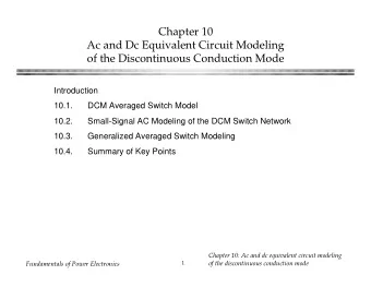
���������������������������������������������� ���������������������������������������������� • Averaged switch model in DCM • Using averaged-switch model to predict converter steady-state characteristics and small-signal dynamics in DCM • Combined CCM/DCM averaged switch model • PSpice implementation of combined CCM/DCM models - ideal switches (ccm-dcm1) - ideal switches in converters with isolation transformer (ccm-dcm2) • Application examples: - comparison of transient simulation results in a SEPIC example using (1) switching circuit model and (2) averaged model - small-signal dynamic responses of a flyback converter operating in CCM or DCM - more converter examples using averaged-switch subcircuits
Change in characteristics at the CCM/DCM boundary Steady-state output voltage becomes strongly load-dependent l Simpler dynamics: one pole and the RHP zero are moved to very high l frequency, and can normally be ignored Traditionally, boost and buck-boost converters are designed to operate l in DCM at full load All converters may operate in DCM at light load l So we need equivalent circuits that model the steady-state and small- signal ac models of converters operating in DCM The averaged switch approach yields an intuitive result that is relatively easy to solve
Derivation of DCM averaged switch model Buck-boost example Switch network • Define switch terminal i 1 i 2 quantities v 1 , i 1 , v 2 , i 2 , as + – shown + v 1 v 2 • Let us find the averaged + v g – + C R v quantities 〈 v 1 〉 , 〈 i 1 〉 , 〈 v 2 〉 , 〈 – i 2 〉 , for operation in DCM, + L v L – and determine the – i L relations between them
DCM waveforms i L (t) i 1 (t) i pk i pk Area q 1 v v g L L i 1 ( t ) T s 0 t v L (t) v g – v v g v 1 (t) v 1 ( t ) T s v g 0 0 v i 2 (t) i pk Area q 2 Switch network i 1 i 2 i 2 ( t ) T s + – + v 1 v 2 v g – v v 2 (t) + v g – + C R v v 2 ( t ) T s – – v + L v L 0 – – i L t d 1 T s d 2 T s d 3 T s T s
Basic DCM equations i 1 (t) Peak inductor current: i pk Area q 1 i pk = v g L d 1 T s i 1 ( t ) T s Average inductor voltage: v g – v v 1 (t) T s + d 3 ⋅ 0 v L ( t ) T s = d 1 v g ( t ) T s + d 2 v ( t ) v 1 ( t ) T s v g 0 In DCM, the diode switches off when the i 2 (t) inductor current reaches zero. Hence, i (0) i pk Area q 2 = i ( T s ) = 0 , and the average inductor voltage is zero. This is true even during i 2 ( t ) T s transients. v L ( t ) T s = d 1 ( t ) v g ( t ) T s + d 2 ( t ) v ( t ) T s = 0 v g – v v 2 (t) v 2 ( t ) T s – v Solve for d 2 : 0 v g ( t ) t T s d 1 T s d 2 T s d 3 T s d 2 ( t ) = – d 1 ( t ) T s v ( t ) T s
Average switch network terminal voltages i 1 (t) Average the v 1 ( t ) waveform: i pk Area q 1 T s = d 1 ( t ) ⋅ 0 + d 2 ( t ) v 1 ( t ) v g ( t ) T s – v ( t ) T s + d 3 ( t ) v g ( t ) T s i 1 ( t ) T s Eliminate d 2 and d 3 : v g – v v 1 (t) v 1 ( t ) T s = v g ( t ) T s v 1 ( t ) T s v g Similar analysis for v 2 ( t ) waveform leads to 0 i 2 (t) i pk Area q 2 T s + d 2 ( t ) ⋅ 0 + d 3 ( t ) – v ( t ) v 2 ( t ) T s = d 1 ( t ) v g ( t ) T s – v ( t ) T s i 2 ( t ) T s = – v ( t ) T s v g – v v 2 (t) v 2 ( t ) T s – v 0 t d 1 T s d 2 T s d 3 T s T s
Average switch network terminal currents Average the i 1 ( t ) waveform: i 1 (t) i pk Area q 1 t + Ts = q 1 T s = 1 i 1 ( t ) i 1 ( t ) dt T s T s i 1 ( t ) T s t The integral q 1 is the area under the i 1 ( t ) waveform during first subinterval. Use triangle v g – v v 1 (t) area formula: v 1 ( t ) T s v g t + Ts = 1 0 q 1 = i 1 ( t ) dt 2 d 1 T s i pk i 2 (t) t i pk Area q 2 Eliminate i pk : 2 ( t ) T s T s = d 1 i 2 ( t ) T s i 1 ( t ) v 1 ( t ) 2 L T s Note 〈 i 1 ( t ) 〉 Ts is not equal to d 〈 i L ( t ) 〉 Ts ! v g – v v 2 (t) v 2 ( t ) T s – v Similar analysis for i 2 ( t ) waveform leads to 2 0 v 1 ( t ) 2 ( t ) T s T s = d 1 T s t i 2 ( t ) d 1 T s d 2 T s d 3 T s 2 L v 2 ( t ) T s T s
Input port: Averaged equivalent circuit i 1 ( t ) T s 2 ( t ) T s T s = d 1 i 1 ( t ) v 1 ( t ) + 2 L T s v 1 ( t ) R e ( d 1 ) v 1 ( t ) T s T s i 1 ( t ) T s = R e ( d 1 ) – R e ( d 1 ) = 2 L 2 T s d 1 Low-frequency components of input port waveforms obey Ohm’s law
Output port: Averaged equivalent circuit i(t) 2 v 1 ( t ) 2 ( t ) T s T s = d 1 + T s i 2 ( t ) 2 L v 2 ( t ) T s p(t) v(t) 2 v 1 ( t ) T s i 2 ( t ) T s v 2 ( t ) T s = R e ( d 1 ) = p ( t ) T s – • Output port is a source of power p ( t ) • Power p ( t ) is independent of load characteristics • Power p ( t ) is dependent on (equal to) the power apparently consumed by the switch network input port
The dependent power source i(t) i(t) + v(t)i(t) = p(t) p(t) v(t) – v(t) • Must avoid open- and short-circuit connections of power sources • Power sink: negative p(t)
How the power source arises in lossless two-port networks In a lossless two-port network without internal energy storage: instantaneous input power is equal to instantaneous output power In all but a small number of special cases, the instantaneous power throughput is dependent on the applied external source and load If the instantaneous power depends only on the external elements connected to one port, then the power is not dependent on the characteristics of the elements connected to the other port. The other port becomes a source of power, equal to the power flowing through the first port A power source (or power sink) element is obtained
Properties of power sources Series and parallel connection of power P 1 sources P 1 + P 2 + P 3 P 2 P 3 n 1 : n 2 Reflection of power source through a transformer P 1 P 1
The loss-free resistor (LFR) i 1 ( t ) T s i 2 ( t ) T s p ( t ) T s + + v 2 ( t ) T s v 1 ( t ) T s R e ( d 1 ) – – A two-port lossless network Input port obeys Ohm’s Law Power entering input port is transferred to output port
Averaged switch model: buck-boost example Switch network i 1 i 2 + – Original circuit + v 1 v 2 + v g – + C R v – + L v L – – i L i 1 ( t ) T s i 2 ( t ) T s p ( t ) T s Averaged model + – + R e (d) v 2 ( t ) T s v 1 ( t ) T s + v g ( t ) T s – + C R v ( t ) Ts – L –
Solution of averaged model: steady state I 1 Let + L → short circuit P C → open circuit + V g R e (D) R V – – Converter input power: 2 Equate and solve: P = V g 2 P = V g R e = V 2 R e R Converter output power: V P = V 2 R V g = ± R e R
Steady-state LFR solution V R V g = ± is a general result, for any system that can R e be modeled as an LFR. For the buck-boost converter, we have R e ( D ) = 2 L D 2 T s Eliminate R e : D 2 T s R V = – D V g = – 2 L K which agrees with the results of previous steady-state analyses.
Averaged models of other DCM converters • Determine averaged terminal waveforms of switch network • In each case, averaged transistor waveforms obey Ohm’s law, while averaged diode waveforms behave as dependent power source • Can simply replace transistor and diode with the averaged model as follows: i 1 ( t ) T s i 2 ( t ) T s i 1 (t) i 2 (t) p ( t ) T s + + + + v 2 ( t ) T s v 1 (t) v 2 (t) v 1 ( t ) T s R e ( d 1 ) – – – –
DCM buck, boost R e = 2 L Buck R e (d) L d 2 T s + v g ( t ) T s + p ( t ) T s v ( t ) Ts C R – – Boost L + v g ( t ) T s + v ( t ) Ts R e (d) C R – p ( t ) T s –
DCM Cuk, SEPIC 2 L 1 || L 2 R e = C 1 Cuk L 1 L 2 d 2 T s + p ( t ) T s + v g ( t ) T s v ( t ) Ts R e (d) C 2 R – – C 1 SEPIC L 1 + p ( t ) T s + v g ( t ) T s v ( t ) Ts R e (d) L 2 C 2 R – –
Steady-state solution: DCM buck, boost Let L → short circuit R e (D) C → open circuit + Buck P + V g R V – – + Boost + V g R e (D) R P V – –
Steady-state solution of DCM/LFR models Converter M, CCM M, DCM 2 Buck D 1 + 1 + 4 R e / R 1 1 + 1 + 4 R / R e Boost 1 – D 2 – D R – Buck-boost, Cuk 1 – D R e D R SEPIC 1 – D R e V g I crit = 1 – D I > I crit for CCM D R e ( D ) I < I crit for DCM
Small-signal ac modeling of the DCM switch network Large-signal averaged model Perturb and linearize: let d ( t ) = D + d ( t ) i 1 ( t ) T s i 2 ( t ) T s v 1 ( t ) T s = V 1 + v 1 ( t ) + p ( t ) T s + i 1 ( t ) T s = I 1 + i 1 ( t ) v 2 ( t ) T s v 1 ( t ) T s R e (d) v 2 ( t ) T s = V 2 + v 2 ( t ) – – i 2 ( t ) T s = I 2 + i 2 ( t ) d(t) 2 ( t ) T s T s = d 1 i 1 = v 1 i 1 ( t ) v 1 ( t ) r 1 + j 1 d + g 1 v 2 2 L T s 2 v 1 ( t ) i 2 = – v 2 2 ( t ) T s T s = d 1 T s r 2 + j 2 d + g 2 v 1 i 2 ( t ) 2 L v 2 ( t ) T s
A more convenient way to model the buck and boost small-signal DCM switch networks i 1 (t) i 1 (t) i 2 (t) i 2 (t) + + + + v 1 (t) v 2 (t) v 1 (t) v 2 (t) – – – – In any event, a small-signal two-port model is used, of the form i 1 i 2 + + v 1 r 1 g 1 v 2 g 2 v 1 r 2 v 2 j 1 d j 2 d – –
Small-signal DCM switch model parameters i 1 i 2 – + v 1 r 1 g 1 v 2 g 2 v 1 r 2 v 2 j 1 d j 2 d – + g 1 j 1 r 1 g 2 j 2 r Switch type 2 1 2(1 – M ) V 1 Buck, 2 – M 2(1 – M ) V 1 M 2 R e R e R e MR e DMR e Fig. 10.16(a) DR e 1 2 2 M – 1 ( M – 1) Boost, ( M – 1) 2 R e 2 MV 1 2 V 1 2 R e R e ( M – 1) 2 R e ( M – 1) M Fig. 10.16(b) D ( M – 1) R e D ( M – 1) R e 2 M Buck-boost, M 2 R e 2 V 1 2 V 1 R e 0 R e Fig. 10.7(b) DR e DMR e
DCM small-signal transfer functions When expressed in terms of R, L, C , and M (not D ), the small- l signal transfer functions are the same in DCM as in CCM Hence, DCM boost and buck-boost converters exhibit two poles l and one RHP zero in control-to-output transfer functions But , value of L is small in DCM. Hence l RHP zero appears at high frequency, usually greater than switching frequency Pole due to inductor dynamics appears at high frequency, near to or greater than switching frequency So DCM buck, boost, and buck-boost converters exhibit essentially a single-pole response A simple approximation: let L → 0 l
The simple approximation L → 0 Buck, boost, and buck-boost converter models all reduce to DCM switch network small-signal ac model + + v g r 1 g 1 v 2 g 2 v 1 r 2 v j 1 d j 2 d C R – – Transfer functions G vd ( s ) = v G d 0 control-to-output = 1 + s G d 0 = j 2 R || r 2 with d ω p v g = 0 1 ω p = R || r 2 C G g 0 G vg ( s ) = v line-to-output = 1 + s G g 0 = g 2 R || r 2 = M v g ω p d = 0
Transfer function salient features ω p G d 0 G g 0 Converter 2 V 1 – M 2 – M Buck M D 2 – M (1 – M ) RC 2 V M – 1 2 M – 1 Boost M D 2 M – 1 ( M – 1) RC V 2 Buck-boost M D RC
DCM boost example Control-to-output transfer function G vd ( s ) D 1 i(t) L i D (t) R = 12 Ω + + v L (t) – i C (t) L = 5 µH + V g Q 1 C R v(t) – C = 470 µF – f s = 100 kHz The output voltage is regulated to be V = 36 V. It is desired to determine G vd (s) at the operating point where the load current is I = 3 A and the dc input voltage is V g = 24 V.
Evaluate simple model parameters P = I V – V g = 3 A 36 V – 24 V = 36 W 2 R e = V g P = (24 V) 2 36 W = 16 Ω 2(5 µ H) 2 L D = = = 0.25 (16 Ω )(10 µ s) R e T s (36 V) (24 V) – 1 2 M – 1 = 2(36 V) G d 0 = 2 V M – 1 = 72 V ⇒ 37 dBV D (0.25) 2 (36 V) (24 V) – 1 2 (36 V) (24 V) – 1 f p = ω p 2 M – 1 2 π = 2 π ( M – 1) RC = = 112 Hz 2 π (36 V) (24 V) – 1 (12 Ω )(470 µ F)
Control-to-output transfer function, boost example 60 dBV ∠ G vd || G vd || G d 0 ⇒ 37 dBV 40 dBV || G vd || f p 20 dBV 112 Hz –20 dB/decade 0 dBV 0˚ 0˚ –20 dBV ∠ G vd –90˚ –40 dBV –180˚ –270˚ 10 Hz 100 Hz 1 kHz 10 kHz 100 kHz f
������������������������������������������� ��������������������� • Observed high-frequency response due to inductor dynamics • Averaged-switch model derivation used: = v 0 L T s which is consistent with the fact that in DCM the inductor current starts from zero and ends at zero in each switching cycle, even in transients • However, high-frequency dynamics due to the inductor indicates that the AC voltage across the inductor in the small-signal model is not zero • Model predictions at high frequencies are not quite correct • Corrected averaged models that include the inductor in the averaged switch model have recently been described See References: [Sun et. al. PESC’99], [Ben-Yaakov et.al. PESC’94]
���������������� �������������������� Objective: a general large-signal averaged-switch model • Valid in CCM and DCM • 5 terminals: transistor port (2 terminals) diode port (2 terminals) duty ratio input (1 terminal) • DCM/CCM boundary resolved within the model, based only on the terminal voltages/currents of the model • Spice compatible
���������������� �������������������� i 1 ( t ) i 2 ( t ) switch 1 3 + + network v 1 ( t ) v 2 ( t ) _ _ 2 4 averaged-switch averaged-switch model model CCM DCM i 1 i 2 i 1 i 2 1 3 1 3 + + + + p ( t ) 1-d 1-d + i 1 v 1 v 2 v 1 v 2 E t G d v 2 R e ( d ) d – d _ _ _ _ 2 4 2 4 5 5 duty duty d d averaged-switch model CCM/DCM i 1 i 2 1 3 + ? v 2 _ _ 2 4 5 duty d
���������������� �������������������� averaged-switch model d , CCM CCM/DCM i 1 i 2 1 3 + + D K = 2 u d 1-u 1-u + i 1 v 1 v 2 E t G d v 2 , DCM – u u i S A + 2 1 d 2 Lf _ _ 2 4 s 5 v 2 duty d 2 d = u MAX d , CCM/DCM boundary: i + 2 1 d 2 Lf s v 2 u = equivalent switch duty ratio
CCM/DCM Averaged-Switch Model PSpice Implementation: ccm-dcm1 ************************************************************************************** * MODEL: ccm-dcm1 * Application: two-switch PWM converters, CCM or DCM * Limitations: ideal switches, no transformer ************************************************************************************** * Parameters: * L=equivalent inductance (relevant for DCM) * fs=switching frequency ************************************************************************************** * Nodes: (same as in ccm1) ************************************************************************************** .subckt ccm-dcm1 1 2 3 4 5 params: L=1 fs=1E6 Et 1 2 value={(1-v(u))*v(3,4)/v(u)} Gd 4 3 value={(1-v(u))*i(Et)/v(u)} Ga 0 a value={MAX(i(Et),0)} Va a b Rdummy b 0 10 Eu u 0 table {MAX(v(5), v(5)*v(5)/(v(5)*v(5)+2*L*fs*i(Va)/v(3,4)))} (0 0) (1 1) .ends **************************************************************************************
���������������� �������������������� �������������������������� averaged-switch model d , CCM CCM/DCM i 1 i 2 1 3 + + = D 2 K u d 1-u i 1 1-u v 2 + , DCM v 1 E t G d v 2 n u – i n u + 2 1 d 2 nLf S A s _ _ v 2 4 5 2 duty d 2 d = u MAX d , CCM/DCM boundary: i + 2 1 d 2 nLf s v 2 u = equivalent switch duty ratio
CCM/DCM Averaged-Switch Model PSpice Implementation: ccm-dcm2 * MODEL: ccm-dcm2 * Application: two-switch PWM converters, CCM or DCM with (possibly) transformer * Limitations: ideal switches, no transformer **************************************************************************************** * Parameters: * L=equivalent inductance (relevant for DCM), referred to primary * fs=switching frequency * n=transformer turns ratio 1:n (primary:secondary) **************************************************************************************** * Nodes: (same as in ccm1) **************************************************************************************** .subckt ccm-dcm2 1 2 3 4 5 params: L=1 fs=1E6 n=1 Et 1 2 value={(1-v(u))*v(3,4)/v(u)/n} Gd 4 3 value={(1-v(u))*i(Et)/v(u)/n} Ga 0 a value={MAX(i(Et),0)} Va a b Rdummy b 0 10 Eu u 0 table {MAX(v(5), v(5)*v(5)/(v(5)*v(5)+2*L*n*fs*i(Va)/v(3,4)))} (0 0) (1 1) .ends ****************************************************************************************
�������������������������� • ccm-dcm1 (for non-isolated converters) and ccm-dcm2 (for converters that may include isolation transformer) are general, large-signal averaged-switch models (PSpice subcircuits) valid for both CCM and DCM • Can be applied to DC, AC, or Transient simulation of any two-switch PWM converter • Limitations: ideal switches, no losses are modeled, but the model can be refined further to include conduction losses • Application examples: • Comparison of Transient simulation results in a Sepic converter example using: – (1) switching circuit model – (2) ccm-dcm2 averaged switch model • AC simulation results for a flyback converter operating in CCM or DCM
Sepic converter example: switching circuit model V L3 R6 C3 23 22x 22 24 800u 0.5 21 Resr3 100u R4 R11 0.2 0.1 20 Vg2 + C4 L4 R5 100u 50V - 100u 100 S2 + + V4 - - + - switch M1 D1 IRF640 R7 MUR820 10 V3 + - Switching frequency 100kHz, duty ratio D=0.5
Sepic converter example: averaged model using ccm-dcm2 V L1 R1 C1 3 2x 2 4 1 800u 0.5 Resr1 R10 100u R2 0.2 0.1 20 Vg + C2 L2 R3 50V 100u - 100u 100 S1 + + V4 - - + U6 - switch D 4 A 1 ccm-dcm2 2 3 K 5 S duty + ACMAG=1V Vd DC=0.5V - Exactly the same PSpice circuit, except the MOSFET M1 and the diode D1 replaced by the ccm-dcm2 subcircuit, and pulsating gate drive V3 replaced by a duty-ratio voltage source Vd
������������������������ ���������������������������� (B) sepic-switch.dat 80V V out Averaged model 60V Switching model 40V start-up transient load transient 20V 0V 0s 5ms 10ms 15ms 20ms V(24) V(4) Time Start-up and load transient response
������������������������ ���������������������������� (B) sepic-switch.dat 10A Diode current during load transient 8A 6A 4A switching model 2A 0A averaged model -2A 10.0ms 10.2ms 10.4ms 10.6ms 10.8ms 11.0ms 11.2ms 11.4ms I(D1) I(X_U6.Gd) Time Details of the diode current waveform around the load transient
Flyback converter example using ccm-dcm2 averaged-switch model T1 1 1 1:n 3 * * PARAMETERS: Lm=50u Rload 2 n=0.25 Lm Vg + 2 4 - 48V transformer R2 V 3 0.2 U1 4 D 4 A 2 1 R1 C1 L=50u ccm-dcm2 500uF {Rload} fs=100K n=0.25 2 3 K 5 S duty AC=1 + Vd 0.25 - CCM for Rload=1 Ohm, DCM for Rload=2 Ohm
������������������������� ������ ccm-dcm2 ���������������������� (C) flyback-ccm-dcm2.dat 50 Magnitude response, control-to-output v/d R load = 1, CCM 0 R load = 2, DCM -50 DB(V(4)) 0d R load = 1, CCM R load = 2, DCM -100d Phase response, control-to-output v/d -200d 10Hz 100Hz 1.0KHz 10KHz 100KHz P(V(4)) Frequency Frequency responses generated by PSpice AC analyses
Other Converter Examples transformer 2 1 Vg Lm + Watkins-Johnson converter - 1:n * * 4 3 transformer 1 D 2 S 2 1 Vg Lm Pspice averaged circuit model ccm-dcm2 + using ccm-dcm2 5 - duty 1:n * * + averaged-switch subcircuit Vd - 4 3 4 3 A K
Other Converter Examples 1 1:n 3 Vg * * + Cuk converter with Lm - isolation transformer 2 4 transformer 1 1:n 3 Vg * * + Lm PSpice averaged circuit model - using ccm-dcm2 2 4 transformer averaged-switch subcircuit U2 D 4 A 1 ccm-dcm2 2 3 K 5 S duty
�������������������������������������������� ������������������������������������� • Averaged switch model for current-programmed mode (CPM) in CCM • Steady-state and simple AC model in CCM • Averaged switch model for CPM in DCM • Steady-state and small-signal AC model in DCM • Large-signal averaged CCM/DCM model for current-mode controller • PSpice implementation of the averaged CPM controller model • Application examples - Buck converter with current-programmed mode controller
Current-programmed control Buck converter L i s (t) i L (t) The peak transistor current + replaces the duty cycle as the Q 1 + v g (t) C v(t) R converter control input. D 1 – – Measure switch i s (t) current Clock Control signal R f i c (t) 0 T s i s (t)R f S Q m 1 Switch current + R i s (t) – Analog Latch i c (t)R f comparator Control Current-programmed controller 0 dT s T s t input Transistor status: on off Clock turns Comparator turns transistor on transistor off Compensator v(t) –+ v ref Conventional output voltage controller
A simple approximation i L ( t ) T s = i c ( t ) • Neglects switching ripple and artificial ramp (slope compensation) • Yields physical insight and simple first-order model • Accurate when converter operates well into CCM (so that switching ripple is small) and when the magnitude of the artificial ramp is not too large • Well-accepted by practicing engineers • Resulting small-signal relation: i L ( s ) ≈ i c ( s )
Averaged switch modeling with the simple approximation Buck converter example L i L (t) i 1 (t) i 2 (t) + + + + v g (t) v 1 (t) C R v(t) v 2 (t) – – – – Switch network Averaged terminal waveforms, The simple approximation: CCM: T s ≈ i c ( t ) v 2 ( t ) T s = d ( t ) v 1 ( t ) i 2 ( t ) T s T s i 1 ( t ) T s = d ( t ) i 2 ( t ) T s
Recommend


More recommend
Explore More Topics
Stay informed with curated content and fresh updates.