A Pulse-Driven VCO with Enhanced Efficiency Aravind Tharayil - PowerPoint PPT Presentation
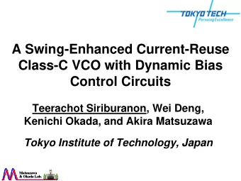
A Pulse-Driven VCO with Enhanced Efficiency Aravind Tharayil Narayanan, Kento Kimura, Wei Deng, Kenichi Okada, and Akira Matsuzawa Tokyo Institute of Technology, Japan b. b. Matsuzawa Matsuzawa & Okada Lab. & Okada Lab. y y
A Pulse-Driven VCO with Enhanced Efficiency Aravind Tharayil Narayanan, Kento Kimura, Wei Deng, Kenichi Okada, and Akira Matsuzawa Tokyo Institute of Technology, Japan b. b. Matsuzawa Matsuzawa & Okada Lab. & Okada Lab. y y
Contents ! Motivation ! Evaluation of VCO Topologies ! Effects of MOSFET Sizing ! Pulse VCO ! Measurement Results ! Conclusion 1
Motivation Low power TRx is required for next gen portable devices 19mA VCO 38% RX 62% 30mA [H. Darabi, JSSC 2011] VCO – A major power consumer in TRx. VCO for next generation wireless devices ! High purity ! High efficiency ! Small area 2
Evaluation of VCO Topologies Generalized expression for phase noise Figure of Merit (FoM) facilitates fair VCO comparison Assuming 100% efficiency and noise free active elements: FoM MAX depends only on Q [A. Hajmiri, JSSC 1998] 3 [M. Garampazzi, ESSCIRC 2014]
Evaluation of VCO Topologies Excess Noise Factor (ENF) ENF = FoM MAX – FoM ENF depends only on topology For high performance VCOs: 1. Increase power efficiency 2. Decrease noise sensitivity 4 [M. Garampazzi, ESSCIRC 2014]
High Efficiency VCOs VDD VDD LDO VDD V P V N V P V N K M V gbias V P V N VDD M1 M2 M1 M2 V Tail M1 M2 V Tail C Tail C Tail M3 M3 Class-C Class-D Class-F High Current High Voltage Low Noise efficiency Efficiency Sensitivity 5 [P. Andreani, JSSC 2008] [L. Fanori, JSSC 2013] [M. Babaie, JSSC 2013]
High Efficiency VCOs ✗ High ! i " Additional area. " Limited improvement. ✗ Low η V η P = η I × η V " Supply pushing. η I : Current efficiecny " Loading effects. η V : Voltage efficiecny " Reliability issues. ✓ High η I " Good candidate for practical high efficiency VCO. [P. Andreani, JSSC 2008] [L. Fanori, JSSC 2013] 6 [M. Babaie , JSSC 2013] [A. Visweswaran, ISSCC 2012]
Tackling Efficiency: Class-C VCO V ds V ds A t V DD V DD V gs V th V gbais V gs - V th −Φ Φ I bias I ds I ds - ϖ 2 - ϖ - ϖ 2 - ϖ ϖ ϖ 2 ϖ ϖ 2 0 0 (a) (b) Class-C achieves high current efficiency 7 [A. Mazzanti and P. Andreani, JSSC 2008]
Efficiency and MOS sizing V DS V DD V TH ! !"# = ! !! − ( ! !" − ! !" ) ! V GS I max1 For high efficiency Φ 1 −Φ 1 I DS1 # Large A max Small MOS I max2 # Small V GS # Small conduction angle −Φ 2 −Φ 2 I DS2 - ϖ - ϖ 0 ϖ ϖ 2 2 Large MOS Large MOS required for better efficiency 8 [K. Okada, VLSI Circuits 2009]
Noise Contribution of MOSFET 20 MOS Noise [dB] 15 10 5 0 ϖ ϖ 0 4 2 Conduction Angle [rad] Low conduction angles increases the noise from MOSFETs 9
Large MOS - Secondary Effects VDD Behavior of C gs C GS V P V N C H C gs C T V gbias C L V TH V DS+TH V GS M1 M2 C gs,M1 C gs,M2 (cut-off) V Tail C Tail (saturation) Tank capacitance is susceptive to V GS variations 10
AM-PM Conversion in Class-C VCO VDD Time Domain Analysis V V P V N V DS V DD C GS V TH V GS ∆ V GS1 ∆ V GS2 -R t C GS Bias ∆ C 1 ∆ C 2 C GS C H t C T f f 0 - Δ f 1 f 0 - Δ f 2 C L δ f -2 ϖ - ϖ 0 ϖ 2 ϖ V GS Variations in C GS translates to phase noise 11
Effects of MOS sizing -90 Phase Noise [dBc/Hz] simula � on including MOS sizing e ff ects -95 excluding MOS sizing e ff ects -100 -105 -110 -115 -0.3 0.0 0.3 0.6 V gbias [V] Lowering V GS worsens the phase noise 12
Pulse Drive: The Concept V A t V ds V DD t 0 V gbias V gs - V th I ds - Φ Φ t - ϖ - ϖ 0 ϖ 2 ϖ 2 Conduction angle is varied by varying gate voltage 13
Pulse Drive: The Concept V A t V ds V DD V gs t 0 I ds −Φ Φ t - ϖ 0 ϖ 2 - ϖ ϖ 2 Conduction angle is controlled by pulse width 14
Noise Contribution of MOSFET 20 MOS Noise [dB] 15 Class-C 10 Pulse VCO 5 0 ϖ ϖ 0 4 2 Conduction Angle [rad] MOSFET noise is kept under limit 15
Theoretical Limit of ENF 20 Class-C Pulse-Drive 15 ENF [dB] 10 5 0 ϖ ϖ 0 4 2 Conduction Angle [rad] Pulse VCO achieves ~5dB improvement in ENF when compared to class-C topology 16
Analysis: AM-PM Conversion VDD Time Domain Analysis V V P V N ∆ V GS1 ∆ V GS2 V DS V DD V TH C GS V GS 0 t -R C GS C T Pulse Drive C L C GS t C H C T f f 0 - Δ f f 0 - Δ f f 0 C L t -2 ϖ - ϖ 0 ϖ 2 ϖ V GS AM-PM translation is minimized. 17
Proposed Circuit Schematic conduction angle VDD control VDD VDD Amplitude V P V N regenerator IB IB R b R b C b C b V bp V bn M1 M2 V Tail M Tail C Tail 18
Pulse Drive: Startup A Tank V DD Cond. Angle Amplitude Control Regeneration V(N B ) ϖ VDD θ N B V Init V bp IB V TH R b C b M b V p Sense Class-AB Class-B Induced Class-C V bp V DD High robustness 0 ϖ t 19 θ
Pulse Drive: Startup Contd . A Tank V DD Cond. Angle Amplitude Control Regeneration V(N B ) ϖ VDD θ N B V Init V bp IB V TH R b C b M b V p Sense Class-AB Class-B Induced Class-C V bp V DD 0 ϖ t 20 θ
Pulse Drive: Steady State A Tank V DD Cond. Angle Amplitude Control Regeneration V(N B ) ϖ θ VDD N B V Init V bp IB V TH R b C b M b V p Sense Class-AB Class-B Induced Class-C V bp V DD High Efficiency 0 ϖ t 21 θ
Chip Micrograph Reference VCO Proposed VDD VDD V P V N V P V N V gbias Pulse Pulse Drive Drive M1 M1 M2 M2 V Tail V Tail C Tail C Tail 250 250 62 45 Pulse Drive 500 500 22
Measurement Results -50 -60 -70 Reference VCO -80 P dc = 2.54mW -90 FoM = -190dBc/Hz -100 -110 This work -120 P dc = 2.05mW -130 FoM = -192dBc/Hz -140 -150 1k 10k 100k 1M 10M • Current implementation limits the maximum achievable frequency. • Spikes in the frequency spectrum can be removed by circuit techniques. 23
Performance Comparison CMOS Frequency Phase Noise Pdc FoM Process [GHz] [dBc/Hz] [mW] [dBc/Hz] [1] JSSC2008 130nm 4.9 -130@1MHz 1.30 -196 [2] VLSI2009 180nm 4.5 -109@1MHz 0.16 -190 [3] JSSC2013 180nm 4.84 -125@1MHz 3.40 -193 [4] ESSCIRC2011 90nm 5.1 -120@1MHz 0.86 -192 [5] JSSC2013 65nm 3.7 -142@3MHz 15.0 -192 [6] JSSC2013 65nm 4.8 -144@10Mhz 4.00 -191 This Work 180nm 3.6 -124@1MHz 2.05 -192 [1] A. Mazzanti and P. Andreani, JSSC 2008. [2] K. Okada et al ., VLSI 2009. [3] W. Deng et al ., JSSC 2013. [4] M. Tohidian et al ., ESSCIRC 2011. [5] M. Babaie et al ., JSSC 2013. [6] L. Fanori et al ., JSSC 2008 24
Conclusion # Techniques for high performance, low power VCOs are briefly introduced. # A performance limiting factor in class-C VCO is identified. # Pulse Bias technique is proposed, which can achieve very high efficiency. # A VCO working on the proposed pulse-bias scheme is presented along with measurement results. 25
APPENDIX 26
Noise from the additional MOS V DS V DD L P C P C CC 0 V P T 1 ISF L P C P τ V N Pulse Generator 0 I DS V DD Delay introduced by the inverter is within safe ISF region. Delay becomes trivial in advanced processes. 27
Noise Contribution V P V N Tank 40 P_Drive P_Drive Noise Contribution (%) N 1 N 2 30 M CC M CC 20 M Tail C Tail V Tail 10 M BIAS VDD IB 0 N 1 R BIAS Misc. M CC M TAIL Tank R BIAS M BIAS C b M b Components V p Noise introduced by the driver circuitry is small. 28
Simulated Waveforms (1) 0.9 6.E-03 0.8 5.E-03 0.7 4.E-03 0.6 Current (A) Voltage (V) 3.E-03 0.5 0.4 2.E-03 0.3 1.E-03 0.2 0.E+00 0.1 0 -1.E-03 3.85E-07 3.85E-07 3.85E-07 3.85E-07 3.85E-07 Time (s) 29
Simulated Waveforms (2) 30
Recommend
More recommend
Explore More Topics
Stay informed with curated content and fresh updates.
