A Potentially Implementable FPGA for Quantum-Dot Cellular Automata - PDF document
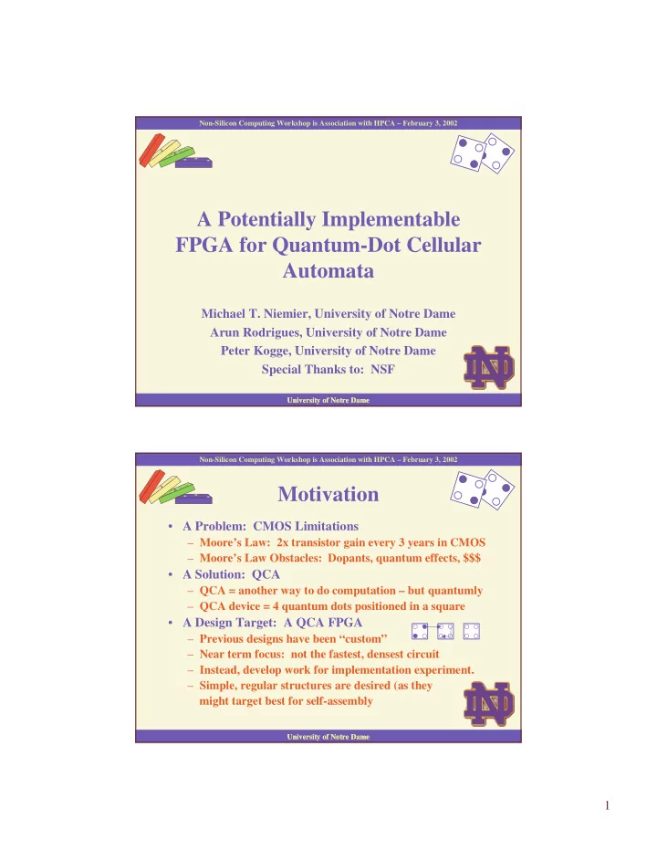
Non-Silicon Computing Workshop is Association with HPCA February 3, 2002 A Potentially Implementable FPGA for Quantum-Dot Cellular Automata Michael T. Niemier, University of Notre Dame Arun Rodrigues, University of Notre Dame Peter Kogge,
Non-Silicon Computing Workshop is Association with HPCA – February 3, 2002 A Potentially Implementable FPGA for Quantum-Dot Cellular Automata Michael T. Niemier, University of Notre Dame Arun Rodrigues, University of Notre Dame Peter Kogge, University of Notre Dame Special Thanks to: NSF University of Notre Dame University of Notre Dame Non-Silicon Computing Workshop is Association with HPCA – February 3, 2002 Motivation • A Problem: CMOS Limitations – Moore’s Law: 2x transistor gain every 3 years in CMOS – Moore’s Law Obstacles: Dopants, quantum effects, $$$ • A Solution: QCA – QCA = another way to do computation – but quantumly – QCA device = 4 quantum dots positioned in a square • A Design Target: A QCA FPGA – Previous designs have been “custom” – Near term focus: not the fastest, densest circuit – Instead, develop work for implementation experiment. – Simple, regular structures are desired (as they might target best for self-assembly University of Notre Dame University of Notre Dame 1
Non-Silicon Computing Workshop is Association with HPCA – February 3, 2002 Where we’ve been Cell 1 (input) Early QCA work mainly devices Cell 1 Cell 4 (input) (device) Cell 3 Cell 5 Progressed to simple (input) (output) circuits, architectures – Simple circuits, µ µ P, our “starting point” µ µ and architectures next logical step 1 1 1 4 3 2 1 4 3 2 1 3 3 3 3 1 2 3 4 1 2 3 4 1 More complex circuits, 1 1 Now, we move on to control logic, and something that can µ Architecture work µ µ µ be built in near-term followed University of Notre Dame University of Notre Dame Non-Silicon Computing Workshop is Association with HPCA – February 3, 2002 The Basics The Device Wire Cross in the Plane P = +1 (Binary 1) P = -1 (Binary 0) 45-Degree Wire Quantum Dot Electron 90-Degree Wire A QCA Wire Proposed experiment – 42 nm Future molecular – 4.2 nm (and room temperature) A 45-degree Wire Majority Gate Signal Propagation Direction Input Cell Cell 1 (input) (frozen polarization) Cell 4 (device) 1 Original signal Cell 1 (input) propagation 2 Cell 5 (output) Complemented Copy Cell 3 (input) University of Notre Dame University of Notre Dame 2
Non-Silicon Computing Workshop is Association with HPCA – February 3, 2002 Experimental QCA • Early and present • 3-input majority logic gate demonstrated work uses “metal” Cell 1 (input) dots Cell 1 Cell 4 (input) (device) • Low temperatures – 70 mK A. Orlov, I. Amlani, G. Bernstein, C. Lent, G. Snider, “Realization Of a functional cell for quantum-dot cellular automata.” Science, 277:928-930, 1997. Cell 3 Cell 5 (input) (output) • QCA wire demonstrated I. Amlani, A. Orlov, G. Toth, G. Bernstein, C. Lent, G. Snider, “Digital logic gate using quantum-dot cellular automata.” Science, 284: 289-291, 1999. • Clocked QCA cells • Single-bit memory demoed demonstrated A. Orlov, I. Amlani, C. Lent, G. Bernstein, G. Snider, “Experimental demonstration of a binary wire for quantum-dot cellular automata.” • Power gain demoed Applied Physics Letters, 74: 2875-77, 1999. • Work underway to • QCA with raise operating temp. chemical molecules A. Orlov, R. Kummamuru, R. Ramasubramaniam, G. Toth, C. Lent, G. Bernstein, G. Snider, “Experimental demonstration of a latch in C. Lent, “Molecular electronics: Bypassing the transistor paradigm.” Clocked quantum-dot cellular automata: Review and recent Science, 288:1597-1599, 2000. Experiments.” J. of Appl. Physics, 85: 4283-85, 1999 University of Notre Dame University of Notre Dame Non-Silicon Computing Workshop is Association with HPCA – February 3, 2002 FPGA Properties Generically, an FPGA = a collection of • S2 S2 functionally complete logic elements S1 S1 0 0 arranged in some interconnection S0 S0 framework SEL SEL A common, unique feature is a pattern • of horizontal and vertical wires with programmable connections for data S2 S2 routing… S1 S1 0 0 S0 S0 • Logic blocks can be connected directly SEL SEL – direct interconnection… …or via long-line interconnect wires • that bypass logic blocks to move a signal “far away” University of Notre Dame University of Notre Dame 3
Non-Silicon Computing Workshop is Association with HPCA – February 3, 2002 The QCA Clock The QCA Clock The CMOS Clock The QCA Clock Phases � The standard CMOS � Cells begin unpolarized clock is signal controlling � Barriers raised, cells “latched” memory transfers Switch � The CMOS clock is 2 � Barriers are held high phases � Used as input to next zone Hold The QCA Clock � Barriers are lowered � Cells relax to unpolarized state � QCA clock not a wire or Release port � Cell barriers remain lowered � QCA “clock” an E-field � Unpolarized, neutral state stays controlling barriers, Relax suppressing e - tunneling � E-field = 4 phase clock University of Notre Dame University of Notre Dame Non-Silicon Computing Workshop is Association with HPCA – February 3, 2002 A Clocking Example “Schematic” Time Step 1 Switch Relax Release Hold Switch Time Step 2 Hold Switch Relax Release Hold Time Step 3 Release Hold Switch Relax Release Time Step 4 Relax Release Hold Switch Relax Time Step 5 Switch Relax Release Hold Switch Clocking Clocking Clocking Clocking Clocking Time Fixed Zone 1 Zone 2 Zone 3 Zone 4 Zone 5 “driver” Wire Position cell University of Notre Dame University of Notre Dame 4
Non-Silicon Computing Workshop is Association with HPCA – February 3, 2002 FPGAs in QCA • The QCA clock scheme results in “inherent self latching” for data movement (i.e. a shift register) • Information transmission is “pipelined” and not instantaneous (unlike CMOS electron flow) • Must coordinate arrival times of signals to logic • Alternative: One big wire in one big clocking zone • Why the alternative doesn’t work: – As a QCA wire grows in length, the probability that all cells will switch successfully decreases University of Notre Dame University of Notre Dame Non-Silicon Computing Workshop is Association with HPCA – February 3, 2002 Switching Matrices and QCA Most useful feature of CMOS FPGA is an easy • means for general purpose interconnect Common method: • – Grid of metal lines (switching matrix) – Junctions = network of pass transistors – North, South, East, or West movement • Pass transistors in CMOS allow current (information) to flow between a and b But in QCA information is moved by nearness , • not e - flow Pass Transistor • No way for pass transistor of only QCA devices University of Notre Dame University of Notre Dame 5
Non-Silicon Computing Workshop is Association with HPCA – February 3, 2002 The QCA Clock and Pass Transistors • The relax clock phase may be the key to the QCA “pass transistor” In the relax phase QCA cells remain • unpolarized so they don’t influence computation • Pass-transistor-esq routing may be accomplished by using the clock to selectively “turn off” groups of QCA cells to create switches Interestingly, a similar technique • may be useful to store data – However, the hold phase would be used to keep data local University of Notre Dame University of Notre Dame Non-Silicon Computing Workshop is Association with HPCA – February 3, 2002 Logic Block Candidates • 3 basic logic blocks considered for initial QCA FPGA: – A block with a single NAND or NOR gate – A block with a programmable majority gate (AND/OR) – A block with some form of memory and logic • Programmable majority gate = sea of AND/OR gates – but no functionally complete logic block! • Block with memory is nice too – but with it (and option 2) programming signal must be routed/stored • Basic NAND gate logic block chosen: – Its functionally complete – Data routing handles all programming – This is first cut so let’s keep it simple, huh? University of Notre Dame University of Notre Dame 6
Non-Silicon Computing Workshop is Association with HPCA – February 3, 2002 An Introduction to Interconnect • Again, in CMOS we usually use SRAM memory to configure pass transistors – But in QCA there are no pass transistors…at least that can be made exclusively of QCA devices… – …and we’re a long way away from a physical SRAM… – …and we want design simplicity • What about multiplexors? – They might offer the most direct translation of CMOS routing techniques to QCA – Simple 2x1 multiplexor/1x2selector could be a pass transistor University of Notre Dame University of Notre Dame Non-Silicon Computing Workshop is Association with HPCA – February 3, 2002 Multiplexors – and why they’re bad Routing Element Area Comparison S AND gate OR gate 1200 1000 A 800 Area 600 Y Anchored 400 200 B 0 1x1 2x2 3x3 Mux AND gate S Routing Element Design Multiplexors require would take at least 6 majority gates! • – This is much bigger than the NAND gate logic block!!! • Also, programming signals would have to be stored/routed University of Notre Dame University of Notre Dame 7
Recommend
More recommend
Explore More Topics
Stay informed with curated content and fresh updates.
