a force of .0059 nN/volt2 per comb-finger height (ym) - PDF document
A High Force Low Area MEMS Thermal Actuator Michael J. Sinclair Microsoft Research Microsoft Corporation ABSTRACT zyxwvutsrqponmlkjihgfedcbaZYXWVUTSRQPONMLKJIHGFEDCBA One Microsoft Way, Redmond, WA 98052 Phone: (425) 703-8343 Fax: (425) 936-7329
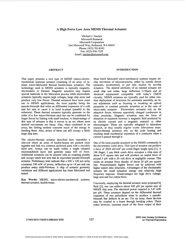
A High Force Low Area MEMS Thermal Actuator Michael J. Sinclair Microsoft Research Microsoft Corporation ABSTRACT zyxwvutsrqponmlkjihgfedcbaZYXWVUTSRQPONMLKJIHGFEDCBA One Microsoft Way, Redmond, WA 98052 Phone: (425) 703-8343 Fax: (425) 936-7329 Email: sinclair@,microsoft.com INTRODUCTION This paper presents a new type of MEMS (micro-electro- Most batch fabricated micro-mechanical systems require on- mechanical systems) actuator consisting of an array of in- chip movement of microstructures, either by outside forces plane micro-fabricated thermal buckle-beam actuators. The (pressure, acceleration) or put into motion by on-chip technology used in MEMS actuators is typically magnetic, actuators. The desired attributes of an intemal actuator are electrostatic or thermal. Magnetic actuators may require small chip real estate, large deflection (>lOpm) and an larger forces by linking with small tendons. zyxwvutsrqponmlkjihgfedcbaZYXWVUTSRQPONMLKJIHGFEDCBA special materials in the fabrication process while electrostatic electrical requirement compatible with today’s CMOS actuators typically require high voltages, large chip areas and circuitry. MEMS actuators are typically used for either one- produce very low forces. Thermal actuators have seen some time deployment of structures for automatic assembly, an in- use in MEMS applications, the most popular being the use adjustment such as focusing or tweaking an optical pseudo-bimorph that relies on differential expansion of a cold parameter or constant periodic actuation as in the case of and hot arm to cause it to bend in-plane (parallel to the micro-optic scanners. Electrostatic actuators rely on the substrate). These thermal actuators typically generate on the attractive forces between oppositely charged conductors in order of a few micro-Newtons each but can be combined for close proximity. Magnetic actuation uses the force of A disadvantage of attraction or repulsion between a magnetic field produced by a force of .0059 nN/volt2 per comb-finger height (ym) zyxwvutsrqponmlkjihgfedcbaZYXWVUTSRQPONMLKJIHGFEDCBA this type of actuator is that it moves in an arc where most an electric current and a magnetic material or other desired movements are linear. Also, when combined in an electromagnet. These are typically relegated to laboratory array, the linking tendons consume much of the energy in research, as they usually require exotic fabrications steps. bending them. Also, arrays of these can still occupy a fairly Electro-thermal actuators rely on the joule heating and large chip area. resulting small mechanical expansion of a conductor when a yields an actuator force density of about 20 zyxwvutsrqponmlkjihgfedcbaZYXWVUTSRQPONMLKJIHGFEDCBA current is passed through it. The electro-thermal actuator described here resembles a chevron where an array of buckle-beams are packed close One of the most popular actuators in the MEMS community is together and link two common anchored arms with a movable the electrostatic comb drive. This type of actuator can produce third arm. Arrays can be made within a single released 113. A micromachined layer and generate many mN of force. 100 finger, 2 pm thick comb drive occupies a chip area of Additional actuators can be arrayed with no coupling penalty about 0.15 square mm and will produce an output force of and occupy much less area that an equivalent pseudo-bimorph around 3 pN with a 50 volt drive at negligible current. This actuator. Preliminary tests indicate that a 450 x 120 pm array pN per square consumes 240 mW of power, deflection up to 14 pm and can mm. Proportionately higher forces can be achieved with produce many milli-Newtons. A chip of actuator geometry higher aspect ratio structures. Advantages of the electrostatic variations and different applications has been fabricated and actuator are small actuation energy and relatively high tested. frequency response. Disadvantages are high drive voltage, large area and low output force. Key Words: MEMS, micro-electro-mechanical systems, thermal actuator, buckle-beam Conversely, employing the thermal actuator array proposed by Reid [2], one can achieve about 450 pN per square mm of MEMS chip area. The electrical power required is 3.87 mW per pN. These actuators depend on the differential thermal expansion of two polysilicon arms to produce a pseudo- bimorph that deflects in an arc. For an array, these devices may be coupled to a beam through bending yokes. These yokes however, consume much of the force output of their 2000 Inter Society Conference 127 0-7803-591 2-7/00/$10.0002000 I E E E on Thermal Phenomena Authorized licensed use limited to: IEEE Xplore. Downloaded on October 21, 2008 at 05:26 from IEEE Xplore. Restrictions apply.
actuators to a common beam produces a linear movement zyxwvutsrqponmlkjihgfedcbaZYXWVUTSRQPONMLKJIHGFEDCBA actuators just in their bending. The coupling of two zyxwvutsrqponmlkjihgfedcbaZYXWVUTSRQPONMLKJIHGFEDCBA per actuator and can produce about zyxwvutsrqponmlkjihgfedcbaZYXWVUTSRQPONMLKJIHGFEDCBA or more - usually desired in MEMS systems. The actuator array presented here consists of only one thermal expansion beam pN 3700 per square mm and 1.53 mW per pN. As structures become more complicated, especially in the case of free-space optical devices [3], the one-time deployment required for assembly becomes more important and reliant on high-force, low-area MEMS Processes (MUMPs) zyxwvutsrqponmlkjihgfedcbaZYXWVUTSRQPONMLKJIHGFEDCBA actuators. Many of the deployment actuators today are of the comb drive type and typically occupy many times the area of (parallel to the substrate). The actuator displacement zyxwvutsrqponmlkjihgfedcbaZYXWVUTSRQPONMLKJIHGFEDCBA the device they are deploying. (I) I' - zyxwvutsrqponmlkjihgfedcbaZYXWVUTSRQPONMLKJIHGFEDCBA d = [ Z2 + 2 zyxwvutsrqponmlkjihgfedcbaZYXWVUTSRQPONMLKJIHGFEDCBA Figure 2. Single buckle-beam actuator. The applied voltage DEVICE FABRICATION causes ohmic heating and expansion between the two fixed anchors, buckling the beam at the midpoint. The tested actuators were fabricated using the Multi-User [4]. MUMPs is a surface d is given micromachining process employing a substrate, an insulating nitride layer and three structural polysilicon layers separated by 1 ~ o s ( a ) ~ - 1 sin(a) by two sacrificial oxide layers as shown in Fig. 1, The second where 1 is the single beam length (buckle-beam half-length) 1.Spm 2.Opm 0.5pm I' is the elongation of the beam due to thermal expansion and a is the pre-bend angle of the beam. the coefficient of thermal expansion used for polysilicon is 2 . 3 3 ~ 1 O-6f'C. The buckle-beam heating temperature was kept below 800 'C to prevent self-annealing which can cause irreversible damage. It should be noted that a buckle-beam can be fabricated out of Figure 1. Cross-section view of the MUMPs fabrication either or both of the MUMPs polysilicon released layers process showing three polysilicon layers with a single anchor giving a possible actuator thickness of 1.5, 2.0 or 3.5 pm. All point. that is required of the fabrication process is that it include at least one releasable layer with a positive temperature and third polysilicon layers (Poly1 and Poly2) are both coefficient of expansion and capable of carrying a current for releasable to act as movable structures. A 0 . 5 pm gold layer ohmic heating. can be pattem-deposited on the Poly2 layer for optical reflection or increased conductivity. The final step performed Arrays of buckle-beam devices can be easily designed by is an HF etch of the intervening sacrificial oxide layers and arranging them in a pattern resembling a chevron as shown in subsequent drying. As is the problem with many MEMS Fig. 3. A center beam is added to stiffen the midpoint and devices, stiction can and does occur between released layers. allow mechanical coupling of the individual beams as well as Movement by the high-force thermal actuators usually releases providing a method of transmitting the linear force to another the offending structure. This is not always the case in stuck device. There is no theoretical limit to the number of beams electrostatic actuators that have to be freed manually. added as long as the device and conductors can handle the current and heat, the beams can lose heat rapidly and there is no cross coupling of heat from one beam to another. Most of ACTUATOR DESIGN the actuator arrays explored in this paper consist of pairs of 218 pm half-beams in varying number and thickness. This The design is based on an in-plane buckle-beam actuator [SI, length was chosen for reasons of published optimum [6] as shown in Fig. 2. As a voltage is applied between the configuration for other thermal actuators using the MUMPS mechanical anchors, ohmic heating of the two half-beams process [2]. causes them to expand and ultimately buckle. The resistivity of polysilicon allows the actuator to operate at voltages and If more than one actuator array is connected (mechanically currents compatible with standard integrated circuitry and electrically) to a single micro-structure, care must be (CMOS). The beam is normally designed with a pre-bend taken to eliminate any common mode currents that arise when angle a so buckling will have an affinity to move in-plane the actuators are excited differently, Fig. 4 shows an 2000 Inter Society Conference 128 on Thermal Phenomena Authorized licensed use limited to: IEEE Xplore. Downloaded on October 21, 2008 at 05:26 from IEEE Xplore. Restrictions apply.
Recommend
More recommend
Explore More Topics
Stay informed with curated content and fresh updates.
