A Brief Intro to Verilog Brought to you by: Sat Garcia Meet your - PDF document
A Brief Intro to Verilog Brought to you by: Sat Garcia Meet your 141(L) TA Sat Garcia sat@cs.ucsd.edu 2 nd Year Ph.D. Student Office Hours: (Tentative) Place: EBU3b B225 (basement) Monday: 3-4pm Wednesday: 11am-Noon
A Brief Intro to Verilog Brought to you by: Sat Garcia Meet your 141(L) TA Sat Garcia sat@cs.ucsd.edu 2 nd Year Ph.D. Student Office Hours: (Tentative) Place: EBU3b B225 (basement) Monday: 3-4pm Wednesday: 11am-Noon Please come to my office hours. I get lonely there by myself! 2 1
What is Verilog? Verilog is: A hardware design language (HDL) Tool for specifying hardware circuits Syntactically, a lot like C or Java An alternative to VHDL (and more widely used) What you'll be using in 141L HELLA COOL!* 3 * If you are totally into hardware design languages Verilog in the Design Process Behavioral Test Algorithm Results Manual Simulate Test Register Results Transfer Level Logic Synthesis Simulate Test Gate Level Results Auto Place + Route Adapted from Arvind & Asanovic’s MIT 6.375 lecture 4 2
Ways To Use Verilog Structural Level Lower level Has all the details in it (which gates to use, etc) Is always synthesizable Functional Level Higher Level Easier to write Gate level, RTL level, high-level behavioral Not always synthesizable We’ll be sticking with functional mostly 5 Data Types in Verilog Basic type: bit vector Values: 0, 1, X (don't care), Z (high impedence) Bit vectors expressed in multiple ways: binary: 4'b11_10 ( _ is just for readability) hex: 16'h034f decimal: 32'd270 other formats but these are the most useful 6 3
Data types (continued) Connect things together with: wire Single wire: wire my_wire; “Array” of wires wire[7:0] my_wire; Why not wire[0:7]? For procedural assignments, we'll use reg Again, can either have a single reg or an array reg[3:0] accum; // 4 bit “reg” reg is not necessarily a hardware register 7 A simple example (comb. circuit) Let's design a 1 bit full adder a b module FA( input a, b, cin, output s, cout); cin assign s = a ^ b ^ c; FA cout assign cout = (a & b) | (a & cin) | (b & cin); endmodule s *** Note: red means new concept, blue and green are just pretty colors :-p Ok, but what if we want more than 1 bit FA? Adapted from Arvind & Asanovic’s MIT 6.375 lecture 8 4
A 4-bit Full Adder We can use 1 bit FA to build a 4 bit full FA FA FA FA adder module 4bitFA( input [3:0] A, B, input cin, output [3:0] S, output cout); wire c0, c1, c2; FA fa0(A[0],B[0],cin,S[0],c0); // implicit binding FA fa1(.a(A[1]), .b(B[1]), .cin(c0), .s(S[1]), .cout(c1)); // explicit binding FA fa2(A[2],B[2],c1,S[2],c2); FA fa3(A[3],B[3],c2,S[3],cout); endmodule Adapted from Arvind & Asanovic’s MIT 6.375 lecture 9 Testing the adder `timescale 1ns/1ns // Add this to the top of your file to set time scale module testbench(); reg [3:0] A, B; reg C0; wire [3:0] S; wire C4; 4bitFA uut (.B(B), .A(A), .cin(C0), .S(S), .cout(C4)); // instantiate adder initial // initial blocks run only at the beginning of simulation (only use in testbenches) begin $monitor($time,"A=%b,B=%b, c_in=%b, c_out=%b, sum = %b\n",A,B,C0,C4,S); end initial begin A = 4'd0; B = 4'd0; C0 = 1'b0; #50 A = 4'd3; B = 4'd4; // wait 50 ns before next assignment #50 A = 4'b0001; B = 4'b0010; // don ’ t use #n outside of testbenches end endmodule 10 5
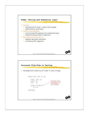
Verilog RTL Operators & ~& | ~| ^ Reduction Arithmetic + - * / % ** ^~ Logical ! && || Shift >> << >>> <<< Relational Concatenation { } > < >= <= == != === Conditional Equality ?: !=== Bitwise ~ & | ^ ^~ Avoid using %, **, and / because you'll run into problems when trying to synthesis Adapted from Arvind & Asanovic’s MIT 6.375 lecture 11 A simple D flip flop (seq. circuit) For sequential circuits, use always blocks Always blocks (and assign) are executed in parallel! module DFF( input clk, d, output q, q_bar); reg q, q_bar; always @ (posedge clk) // triggered on the rising edge of the clock begin q <= d; // non-blocking assignment (LHS not updated until later) q_bar <= ~d; /* q_bar <= ~q will not function correctly! */ end endmodule Adapted from Arvind & Asanovic’s MIT 6.375 lecture 12 6
Always blocks in comb. circuits Can use continual assignment AND always blocks for combinational circuits Our 1-bit adder using always block module FA( input a, b, cin, output s, cout); reg s, cout; // when using always block, LHS must be reg type always @ ( a or b or cin ) // for comb circuits, sensitive to ALL inputs begin s = a ^ b ^ cin; // use blocking assignment here (LHS immediately) cout = (a & b) | (a & cin) | (b & cin); end endmodule 13 Quick Note on blocking vs. non- blocking Order of blocking statements matter These are not the same c = a + b; d = c + e; d = c + e; c = a + b; Order of non-blocking statements doesn’t These are the same d <= c + e; c <= a + b; c <= a + b; d <= c + e; Use non-blocking with sequential, blocking with combintational 14 7
Tips for maintaining synthesizability Only leaf modules should have functionality All other modules are strictly structural, i.e., they only wire together sub-modules Use only positive-edge triggered flip-flops for state Do not assign to the same variable from more than one always block Separate combinational logic from sequential logic Avoid loops like the plague Use for and while loops only for test benches Adapted from Arvind & Asanovic’s MIT 6.375 lecture 15 Another Example (4 input MUX) We can use case module mux4( input a, b, c, d, statements within input [1:0] sel, output out ); an always block reg out; always @( * ) begin case ( sel ) 2’d0 : out = a; 2’d1 : out = b; 2’d2 : out = c; 2’d3 : out = d; default : out = 1’bx; endcase end endmodule Adapted from Arvind & Asanovic’s MIT 6.375 lecture 16 8
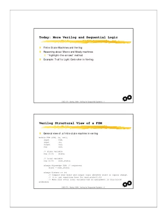
Finite State Machines (FSMs) Useful for designing many different types of circuits 3 basic components: Combinational logic (next state) Sequential logic (store state) Output logic Different encodings for state: Binary (min FF’s), Gray, One hot (good for FPGA), One cold, etc 17 A simple FSM in Verilog module simple_fsm( input clk, start, output restart); reg [1:0] state, next_state; parameter S0 = 2’b00, S1 = 2’b01, S2 = 2’b10; // binary encode always @ (*) begin : next_state_logic case ( state ) S0: begin if ( start ) next_state = S1; else next_state = S0; end // continued from left S1: begin next_state = S2; end always @ (posedge clk) S2: begin begin: state_assignment if (restart) next_state = S0; state <= next_state; else next_state = S2; end end endmodule default: next_state = S0; endcase end // continued to the right 18 9
Tips on FSMs Don’t forget to handle the default case Use two different always blocks for next state and state assignment Can do it in one big block but not as clear Outputs can be a mix of combin. and seq. Moore Machine: Output only depends on state Mealy Machine: Output depends on state and inputs 19 Next step: design your own HW Now that you have the basics… Check out MIT’s 6.375 course webpage Thanks to Asanovic & Arvind for slides Lectures 2 and 3 on Verilog http://csg.csail.mit.edu/6.375/handouts.html Try making some simple circuits Beware when Googling for “verilog tutorial” A lot of code out there isn’t synthesizable 20 10
Recommend
More recommend
Explore More Topics
Stay informed with curated content and fresh updates.
