432 This slide shows various possibilities in which etching can be - PDF document
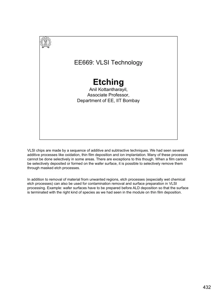
VLSI chips are made by a sequence of additive and subtractive techniques. We had seen several additive processes like oxidation, thin film deposition and ion implantation. Many of these processes cannot be done selectively in some areas. There are
VLSI chips are made by a sequence of additive and subtractive techniques. We had seen several additive processes like oxidation, thin film deposition and ion implantation. Many of these processes cannot be done selectively in some areas. There are exceptions to this though. When a film cannot be selectively deposited or formed on the wafer surface, it is possible to selectively remove them through masked etch processes. In addition to removal of material from unwanted regions, etch processes (especially wet chemical etch processes) can also be used for contamination removal and surface preparation in VLSI processing. Example: wafer surfaces have to be prepared before ALD deposition so that the surface is terminated with the right kind of species as we had seen in the module on thin film deposition. 432
This slide shows various possibilities in which etching can be done. We would look at the terminology in greater detail. 433
When a material is being etched through a mask, the etching can happen vertically in the opening in the mask as well as laterally under the mask as shown. In a fully directional etch, the lateral etch rate would be zero. B is called the etch bias. When etching happens in all directions in equal measure, we have isotropic etching. When the etching happens only vertically, the etching is called anisotropic. 434
435
The etch rate and selectivity depends on the concentration, temperature and stirring conditions. Some of the factors that we need to consider in some detail are the following: As the chemical reaction happens, we may reasonably assume that the liquid next to the surface would be depleted of reactants. The surface is being etched. So some chemical reaction is happening and the reaction products should be either soluble or gases. The reaction products have to be removed from the surface. Stirring of etching solutions helps to enhance etch rates and improve uniformity as the products of reactions would be taken away more efficiently with stirring. Stirring the solution avoids redeposition of particles lifted from the wafer surface and also result in rapid replenishment of the reactants at the wafer surface. 436
Detailed etch processes and rates under typical conditions are documented in: 1. Kirt R. Williams and Richard S. Muller, Etch Rates for Micromachining Processing, IEEE JOURNAL OF MICROELECTROMECHANICAL SYSTEMS, VOL. 5, NO. 4, pp. 256-269, DECEMBER 1996 2. Kirt R. Williams, Kishan Gupta, and Matthew Wasilik, Etch Rates for Micromachining Processing – Part II, IEEE JOURNAL OF MICROELECTROMECHANICAL SYSTEMS, VOL. 12, NO. 6, pp DECEMBER 2003 The overall chemical reaction proposed is shown. Etch rate of the oxide vary with the doping, density and stoichiometry. For example a thermal CVD or PECVD SiO 2 generally etch faster than a thermal oxide. Even though nitride may not be etched as fast as oxide, this again depends on the composition. Thermal CVD nitride etches slow in HF and PECVD nitride may etch faster depending on the density, oxygen and hydrogen content in the film. Typical selectivity of the SiO 2 etch to Si 3 N 4 are in the range of 20 to 100. Buffered HF (BHF) is a mixture of HF and NH 4 F. Typical mixture is 1 part by weight of 49% weight percent HF and 5 parts by weight of 40 weight percent NH 4 F. So the solution would contain 33% percent by weight of NH 4 F and 8.3% percent by weight of HF. One advantage of BHF is that it does not attack photo resist. However HF attacks resist. The BHF reaction is expected to be along the lines shown at the bottom. It is assumed that the NH 4 F reacts to form NO 2 which subsequently oxidizes the silicon and the oxide is then etched by HF. 437
438
439
N(CH 3 ) 4 OH is tetra methyl ammonium hydroxide (TMAH). These hydroxies etch the (100) and (110) planes of Si faster than (111)440 planes. 440
441
442
443
444
445
446
447
448
449
450
451
452
453
454
455
Recommend
More recommend
Explore More Topics
Stay informed with curated content and fresh updates.
