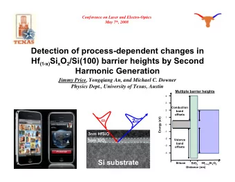
1,2 Y. Q. An, 1 M. C. Downer 1 J. Price, 1 The university of - PowerPoint PPT Presentation
Understanding process-dependent oxygen vacancies in thin HfO 2 /SiO 2 stacked-films on Si (100) via competing electron-hole injection dynamic contributions to second harmonic generation. 1,2 Y. Q. An, 1 M. C. Downer 1 J. Price, 1 The
Understanding process-dependent oxygen vacancies in thin HfO 2 /SiO 2 stacked-films on Si (100) via competing electron-hole injection dynamic contributions to second harmonic generation. 1,2 Y. Q. An, 1 M. C. Downer 1 J. Price, 1 The university of Texas at Austin, Department of Physics, Austin, TX 2 SEMATECH, Austin, TX
Abstract: Optical Second Harmonic Generation (SHG) is used to characterize charge trapping dynamics in thin HfO 2 films deposited on chemically oxidized P-type Si(100) substrates. Previous work identified Electrostatic Field Induced Second Harmonic (EFISH) generation as the dominant process-dependent contribution to the nonlinear response of such structures. EFISH generation was attributed to charges trapped primarily in oxygen vacancy defects located at the SiO 2 /HfO 2 interface that create an electrostatic field acting on the silicon space charge region. Here, we extend the understanding of charge trapping by monitoring SHG as HfO 2 thickness and post- deposition anneal (PDA) temperature are modified. Corresponding trends in time- dependent SHG are identified that reflect unique contributions from competing electron and hole injection dynamics. Specifically, we attribute the initial increase in Time Dependent (TD) SHG intensity to photo-excited electrons from the silicon dominating the electrostatic field response. The subsequent decrease in SHG intensity corresponds to the resonant tunneling of hole carriers trapped at the interface and creating a larger field but biased in the reverse direction of the initial dipole field located at the interface. These results show that SHG can provide an in situ , non-destructive diagnostic of charge trapping in thin gate dielectric films. Key take-home points: • TD SHG governed by both electron and hole injection dynamics: - Photo-excited electrons cause increase in SHG - Trap-assisted hole tunneling causes decrease in SHG • Density of charge trapping defects in the gate dielectric will promote charge transfer and build up of interfacial electric field • SHG provides the ability to qualitatively understand gate oxide and interface integrity due to charge trapping defects
High- k dielectric defects and device performance: • What are they? Anything that can trap charges. - O 2 , N 2 , vacancies and / or interstitials. - Impurities (C, B, etc.). - Crystal imperfections (grain boundaries, surface states). - All are discrete localized states within the band gap. • How does this affect device performance? - Degradation of carrier mobility. - Charge trapping. - increase in leakage current. 4 10 350 SiO 2 2.0nm HfO 2 2 ] 2 Current Density [-A/cm 10 300 Mobility (cm 2 /V-s) 0 10 250 2nm -2 10 200 3nm 3.0nm HfO 2 -4 10 150 -6 10 100 4nm 4.0nm HfO 2 -8 10 50 -10 10 0 0 1 2 3 4 5 6 0.0 0.5 1.0 1.5 2.0 2.5 Voltage [-V] Electric Field (MV/cm) P. D. Kirsch et al. J. Appl. Phys. 99, 023508 (2006)
Previous results: Rotational anisotropic SHG : 4nm HfO 2 Normalized SHG intensity (arb. units) 0.20 0.19 High- κ 0.18 0.17 0.16 + + + + + + + + + + SiO 2 interfacial layer 0.15 0.14 0.13 Si Substrate 0 50 100 150 200 250 300 350 Azimuthal angle ( φ ) 2 ω = + ( ϕ Spectroscopic SHG ( 2 ) PP PP I a a Cos 4 ) 4nm SHG E 1 resonance PP 0 4 indicative of EFISH. 2nm 0.45 • PP is from silicon, but very weak a 4 No E 1 resonance 0.40 usually observed without a DC field 0 0 0.35 present. − = + + 0.30 Si SiO SiO High k PP / / Si a a a a 2 2 0 0 0 EFISH 0.25 EFISH Si a 0.20 Previous work demonstrated these two coefficients are negligible. 0.15 ∴ ≠ Si 0.10 a 0 • (Dominant contribution) EFISH 0.05 E lectric F ield I nduced S econd H armonic G eneration (EFISH). 2.9 3.0 3.1 3.2 3.3 3.4 Photon Energy (eV) R. Carriles, et. al., Appl. Phys. Lett., 88 , 161120 (2006),
Varying Composition: Varying Anneal Temperature: What did we learn? � Interfacial electrostatic fields are primary contribution to SHG response. � These interfacial fields are modified by subtle film growth conditions (composition, anneal temperature, and thickness). � Photo-excited charge carriers in the substrate, trapped in the dielectric defect centers, are the source of these DC field. R. Carriles, et. al., JVST B, 24 , 2160 (2006)
SHG measurements: ω ω ω = χ ( 2 ) ( 2 ) ( ) ( ) P E E • Second Harmonic Generation: i ijk j k χ = χ ≠ χ ≠ ( 2 ), bulk ( 2 ), surface ( 2 ), EFISH • Symmetry arguments govern SHG: 0 0 0 , , ijk ijk ijk Blue Glass 2 ω ∝ χ + χ ω 2 ( 2 ) ( 3 ) 2 • TD-SHG: Analyzer Filter I ( t ) E ( t ) I ( ) DC PMT Half-waveplate Red Glass Thin film (only for S-in) Filter polarizer Sample f f=10cm, Au spherical Rotational Mirror Stage PMT Blue Computer Z-cut Glass Filter Quartz Laser 30 fs, 1nJ Normalization Arm 750 nm
Samples: • HfO 2 deposited via Atomic Layer Deposition (ALD). • Interfacial oxide thickness previously determined using HR-TEM. • HfO 2 thickness verified using spectroscopic ellipsometry. • Post Deposition and Rapid Thermal Anneals (PDA & RTA) performed ex-situ . Objective : Investigate the evolution of HfO 2 crystallinity, bottom interfacial layer stoichiometry, and charge trap defect density as a function of thickness and anneal.
Anatomy of a time dependent SHG measurement: 3 possible charge transfer mechanisms: Electrons diffuse 1. Photo-excited electron injection: 4.3 eV • Si / SiO 2 band offsets = 4.3 eV. Therefore, 3 photon e + (h ν = 1.6 eV) process necessary to inject electrons. Si SiO 2 HfO 2 2. Photo-excited hole injection: e - • Si / SiO 2 band offsets = 5.8 eV. Therefore, 4 photon (h ν = 1.6 eV) process necessary to inject holes. 5.8 eV 3. Trap-assisted resonant tunneling: Electrons or holes can tunnel through ~ 1nm interfacial layer. Holes diffuse E-field breaks translational symmetry and enhances SHG response t > 0 t >> 0 t = 0 750 nm 750 nm 375 nm 375 nm 2 ω ω ω 2 ω e - e - e - e - e - e - e - e - e - e - e - Oxide E dc E dc Si substrate Si substrate Si substrate
Time Dependent SHG: As-deposited HfO 2 0.30 2 nm SHG time evolution: Normalized SHG intensity (A. U.) 0.28 • t < 15sec: SHG increases due to photo-excited 0.26 electrons creating a stronger Initial built-in interfacial electrostatic field. Thicker samples have a 0.24 dipole field value stronger interfacial field • t ~ 15sec: SHG reaches a 3 nm causing decrease in 0.22 maxima due to competing SHG due to more bulk Beam blocked electron/hole created fields defects in the HfO 2 0.20 equally opposing each promoting trap assisted hole tunneling. other. 0.18 • t > 15sec: SHG decreases due to resonant tunneling 0.16 4 nm hole carriers dominating the build up of interfacial fields. 0.14 λ = 750 nm • t = 210-440sec: dark 0.12 period, system recovery. power = 250mW • t > 440sec: 3nm and 4nm 0 100 200 400 500 Time (sec) HfO 2 SHG signals still dominated by resonant hole t < 15 t > 15 t ~ 15 tunneling dynamics. 2nm e - e - e - e - e - e - e - e - e - e - e - e - HfO 2 SHG signal increases e - e - e - e - e + e + e + e + e + e + e + e + e + e + e + e + e + e + e + e + due to photo-excited electron injection. Si substrate Si substrate Si substrate
Time Dependent SHG: annealed HfO 2 0.30 4 nm SHG time evolution: 3 nm Normalized SHG intensity (A. U.) 2 nm • t < 160sec: SHG increases to a saturated intensity value due to photo- excited electrons creating a 0.25 stronger interfacial electrostatic field. • t = 160-225sec: dark period, system recovery. • t > 225sec: 3nm and 4nm HfO 2 SHG signals 0.20 monotonically rise to a beam saturated intensity. 2nm blocked HfO 2 SHG signal unexpectedly decreases to λ = 750 nm the same saturated intensity power = 250mW value. 0 50 100 150 250 300 Time (sec) No decrease in SHG is observed for the annealed samples, corresponding to reversal of the interfacial electrostatic field, presumably due to less bulk defects available to promote trap assisted hole tunneling. Therefore, dominant charge transfer mechanism is photo-excited electron transfer to the surface.
Rotational Anisotropic SHG: As- deposited 4nm HfO 2 0.2 3nm HfO 2 2nm HfO 2 0.5 0.1 -50 0 50 100 150 200 250 300 350 400 700C Anneal a 0 (arb. units) 0.20 0.15 0.20 -50 1000C anneal 0 50 100 150 200 250 300 350 400 0.4 0.15 As-deposited 700C, NH3 1000C, NH3 0.10 50 100 150 200 250 300 350 • Previous studies indicated dipolar coefficient’s (a 0 ) main contribution from EFISH. • Except for the 4nm 700C sample, a 0 trends inversely with temperature and thickness. • RA-SHG results indicate that EFISH contribution from charge trap centers is sensitive to both changes in temperature and film thickness.
Recommend
More recommend
Explore More Topics
Stay informed with curated content and fresh updates.


