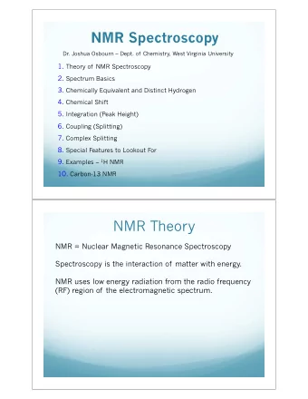
Xray photoelectron spectroscopy An introduction Spyros Diplas - PowerPoint PPT Presentation
Xray photoelectron spectroscopy An introduction Spyros Diplas spyros.diplas@sintef.no spyros.diplas@smn.uio.no SINTEF Industry, Materials Physics -Oslo & Centre of Materials Science and Nanotechnology, Department of Chemistry, UiO
X‐ray photoelectron spectroscopy ‐ An introduction Spyros Diplas spyros.diplas@sintef.no spyros.diplas@smn.uio.no SINTEF Industry, Materials Physics -Oslo & Centre of Materials Science and Nanotechnology, Department of Chemistry, UiO 1
Material Characterisation Methods 2
What is surface? • What happens at surfaces is extremely important in a vast range of applications from environmental corrosion to medical implants. • A surface is really the interface between different phases (solid, liquid or gas). • We can think of the surface as the top layer of atoms but in reality the state of this layer is very much influenced by the 2 – 10 atomic layers below it (~0.5 – 3 nm). • Surface modification treatments are often in the range of 10 – 100 nm thick. >100 nm can be thought of as the bulk. • Surface analysis encompasses techniques which probe the properties in all these ranges. God made solids, but surfaces were the work of the devil ------Wolfgang Pauli 3
Surface Analysis ‐ Techniques Available • Properties and reactivity of the surface will depend on: • bonding geometry of molecules to the surface • physical topography photons EXCITATION EMISSION • chemical composition ions • chemical structure • atomic structure electrons • electronic state Interaction with material No one technique can provide all these pieces of information. However, to solve a specific problem it is seldom necessary to use every technique available. TRANSMISSION 4
XPS‐Basic Principle Photoelectron Auger electron Vacuum Fermi valence band 2p 1/2 , 2p 3/2 L 23 2s L 1 Internal transition hν (irradiative) 1s K E kin = h ν – E B - E KL2,3L2,3 (Z) = E K (Z) – [E L2,3 (Z) + E L2,3 (Z + 1)] Excitation De-excitation An XPS spectrum consists of peaks corresponding to emission of both photoelectrons and Auger electrons 5
Auger electron vs x‐ray emission yield 1.0 Auger Electron Emission 0.8 Probability 0.6 0.4 0.2 X‐ray Photon Emission 0 5 10 15 20 25 30 35 40 Atomic Number B Ne P Ca Mn Zn Br Zr Elemental Symbol 6
Schematic of an XPS spectrometer Hemispherical Electron energy electrodes analyser Slit Slit X-ray source Electrostatic Al electron lens Electron detector e - Photon Sample Number of emitted electrons measured as function of their kinetic energy 7
Examples of XPS spectrometers 8
Instrument: Kratos Axis Ultra DLD at MiNaLab Analyser Detector e - e - Monochromator X-ray source X-ray source Sample 9
Why is XPS surface sensitive? Typical electron energies in XPS Depth of Analysis the XPS spectrum The probability that a photoelectron will escape from the sample without losing energy is regulated by the Beer‐Lambert law: Where λ e is the photoelectron inelastic mean free path Attenuation length (λ) ≈0.9 IMFP IMFP: The average distance an electron with a given energy travels between successive inelastic collisions 10
Features of the XPS spectrum Primary structure - Core level photoelectron peaks (atom excitation) - Valence band spectra - CCC, CCV, CVV Auger peaks (atom de-excitation) Secondary structure - X-ray satellites and ghosts - Shake up and shake off satellites - Plasmon loss features - Background (slope) 11
XPS spectrum ITO Photoelectron peaks x 104 Sn 3d 80 Auger peaks In 3d O 1s Sn 3p 70 In 3p In 3s 60 In 3s 50 S Sn MNN P C 40 In MNN In/Sn 4s 30 O KLL In/Sn 4p 20 C 1s 10 1200 1000 800 600 400 200 0 Binding Energy (eV) 12
Peak width ( ΔE) 2 + ΔE p 2 + ΔE a ΔE = (ΔE n 2 ) 1/2 Analyser contribution Natural width X-ray source contribution Gaussian broadening: -Instrumental: There is no perfectly resolving spectrometer nor a perfectly monochromatic X-ray source. -Sample: For semiconductor surfaces in particular, variations in the defect density across the surface will lead to variations in the band bending and, thus, the work function will vary from point to point. This variation in surface potential produces a broadening of the XPS peaks. -Excitation process such as the shake-up/shake-off processes or vibrational broadening. Lorentzian broadening: The core-hole that the incident photon creates has a particular lifetime (τ) which is dependent on how quickly the hole is filled by an electron from another shell. From Heisenberg’s uncertainty principle , the finite lifetime will produce a broadening of the peak. Γ=h/τ Intrinsic width of the same energy level should increase with increasing atomic number 13
Chemical shift ΔE (i) = kΔq + ΔV M – ΔR final state contribution Initial state contribution • ΔR: relaxation energy change arising from • Δq: changes in valence charge the response of the atomic environment (local electronic structure) to the screening of the core hole • ΔV M : Coulomb interaction between the photoelectron (i) and the surrounding charged atoms. . 14
Chemical shift - Growth of ITO on p c-Si Si In oxide Sn oxide In3d Si2p Sn3d Si 2p Sn 3d 5/2 In 3d 5/2 Intensity arbitrary units 3/2 3/2 In Sn 3.0 nm 3.0 nm SiO x 3.0 nm 3.0 nm 1.5 nm 1.5 nm 1.5 nm 1.5 nm 1.5 nm 1.5 nm 0.5 nm 0.5 nm 0.5 nm 0.5 nm BHF 15 sec + 500 o C 0.5 nm BHF 15 sec + 500°C 0.5 nm 104 102 100 98 456 454 452 450 448 446 444 442 440 500 495 490 485 480 Binding Energy (eV) 15
Chemical shift 16
Quantification Unlike AES, SIMS, EDX, WDX there are little in the way of matrix effects to worry about in XPS. We can use either theoretical or empirical cross sections, corrected for transmission function of the analyser. In principle the following equation can be used: I = J ρ σ K λ I is the electron intensity J is the photon flux, ρ is the concentration of the atom or ion in the solid, σ s is the cross-section for photoelectron production (which depends on the element and energy being considered), K is a term which covers instrumental factors, λ is the electron attenuation length. In practice atomic sensitivity factors (F) are often used: [A] atomic % = {(IA/FA)/Σ(I/F)} Various compilations are available. 17
Spin-Orbit Coupling/Splitting 2p 3/2 Ti oxide 2p The intensity of Arbitrary Units the peaks is given 2p 1/2 by the degeneracy g J = 2j+1 468 466 464 462 460 458 456 Binding Energy (eV) Spin-orbit coupling/ splitting: final state effect for orbitals with orbital angular momentum l> 0. A magnetic interaction between an electron’s spin and its orbital angular momentum. Example Ti. Upon photoemission an electron from the p orbital is removed - remaining electron can adopt one of two configurations: a spin-up (s=+1/2) or spin-down (s=-1/2) state. If no spin-orbit interaction these two states would have equal energy (degenerated states). spin-orbit coupling lifts the degeneracy To realise that we need to consider the quantum number, j , the total angular momentum quantum number . j = l + s where s is the spin quantum number (±½). For a p orbital j=1/2 or 3/2. Thus the final state of the system may be either p1/2 or p3/2 and this gives rise to a splitting of the core-level into a doublet as shown in the figure above. Spin-orbit coupling is described for light elements by the Russell-Saunders ( LS ) coupling approximation and by the j-j coupling approximation for heavier elements 18
Depth profile with ion sputtering SnO 2 Sn Use of an ion gun to erode the sample surface and re-analyse Enables layered structures to be investigated Investigations of interfaces Depth Depth resolution improved by: 500 496 492 488 484 480 Low beam energies Small ion beam sizes Sample rotation 19
Elemental distribution and oxygen deficiency of magnetron sputtered ITO films A. Thøgersen, M.Rein, E. Monakhov, J. Mayandi, S. Diplas JOURNAL OF APPLIED PHYSICS 109, 113532 (2011) In‐oxide In ITO surface ITO/Si interface 20
XPS-Check list Depth of analysis ~ 5nm All elements except H and He Readily quantified (limit ca. 0.1 at%) All materials (vacuum compatible) Chemical/electronic state information - Identification of chemical states - Reflection of electronic changes to the atomic potential Compositional depth profiling by -ARXPS (ultra thin film <10 nm), -change of the excitation energy -choose of different spectral areas -sputtering Ultra thin film thickness measurement Analysis area mm 2 to 10 micrometres 21
Recommend
More recommend
Explore More Topics
Stay informed with curated content and fresh updates.

