UMBC A B M A L T F O U M B C I M Y O R T 1 - PowerPoint PPT Presentation
Advanced VLSI Design Basics CMPE 640 MOS: Metal-Oxide-Silicon Metal gate has been replaced by polysilicon or poly in todays processes. Poly is used as a mask to allow precise definition of the source and drain regions. Minimizes
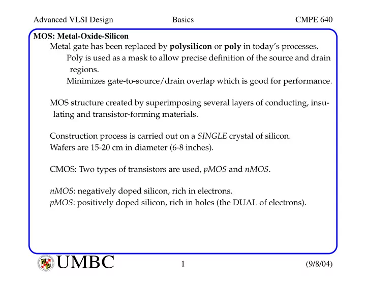
Advanced VLSI Design Basics CMPE 640 MOS: Metal-Oxide-Silicon Metal gate has been replaced by polysilicon or poly in today’s processes. Poly is used as a mask to allow precise definition of the source and drain regions. Minimizes gate-to-source/drain overlap which is good for performance. MOS structure created by superimposing several layers of conducting, insu- lating and transistor-forming materials. Construction process is carried out on a SINGLE crystal of silicon. Wafers are 15-20 cm in diameter (6-8 inches). CMOS: Two types of transistors are used, pMOS and nMOS . nMOS : negatively doped silicon, rich in electrons. pMOS : positively doped silicon, rich in holes (the DUAL of electrons). L A N R Y D UMBC A B M A L T F O U M B C I M Y O R T 1 (9/8/04) I E S R C E O V U I N N U T Y 1 6 9 6
Advanced VLSI Design Basics CMPE 640 An nMOS transistor R s R d V DS V GS I DS I DS GND W Gate Source Drain L Thin Oxide n-channel Drain Source n+ n+ GND p-substrate diffusion L A N R Y D UMBC A B M A L T F O U M B C I M Y O R T 2 (9/8/04) I E S R C E O V U I N N U T Y 1 6 9 6
Advanced VLSI Design Basics CMPE 640 Inverter Cross-section (Out) p-substrate contact m1-m2 contact p-diffusion contact (source) m2 m1 n-substrate contact n-diffusion contact (source) glass V DD GND layer #3 layer #2 layer #1 p+ n+ p+ n+ p+ n+ n-well (drains) p substrate n-transistor p-transistor polysilicon gate (In) L A N R Y D UMBC A B M A L T F O U M B C I M Y O R T 3 (9/8/04) I E S R C E O V U I N N U T Y 1 6 9 6
Advanced VLSI Design Basics CMPE 640 MOS Transistors as Switches We can treat MOS transistors as simple on-off switches with a source (S), gate (G) (controls the state of the switch) and drain (D). Let ‘1’ represent high voltage: typically V DD < 2.0V. Let ‘0’ represent low voltage: GND or V SS . Signals such as ‘1’ and ‘0’ have strength , measures their ability to: • Sink (to lower voltage, e.g. GND) or • Source (from higher voltage, e.g. V DD ) current. n MOS and p MOS signal transmission strength: G 1 G 0 S D S D *** Strong *** Weak 0 0 n MOS p MOS 0 1 Weak *** Strong *** 1 1 L A N R Y D UMBC A B M A L T F O U M B C I M Y O R T 4 (9/8/04) I E S R C E O V U I N N U T Y 1 6 9 6
Advanced VLSI Design Basics CMPE 640 MOS Transistor Switches The reason p-transistors are poor transmitters of logic 0 and n-transistors are poor transmitters of logic 1 is related to threshold voltage (V t ~= 500mV). Threshold voltage will be discussed in detail soon. Under the “switch” abstraction, G has complete control and S and D have no effect. In reality, the gate can turn the switch on only if a potential difference of at least V t exists between the G and S. This is clearly not the case for the “weak” bias configurations and “weak” 0s (~V t ) and “weak” 1s (~V DD -V t ) result. Therefore, the following buffer implementation is a bad idea. A V DD BAD IDEA P1 N1 Out L A N R Y D UMBC A B M A L T F O U M B C I M Y O R T 5 (9/8/04) I E S R C E O V U I N N U T Y 1 6 9 6
Advanced VLSI Design Basics CMPE 640 MOS Transistor Switches The off state of a transistor creates a high impedance condition Z at the drain. No current flows from source to drain: drain source source drain 0 1 Z Z p MOS n MOS Complementary Switch or transmission gate or pass gate : A One p MOS and one n MOS in parallel. Note that neither transistor is connected P1 to V DD or GND. In Out A and A control the transmission of a N1 signal on In to Out . A This configuration allows ‘1’s and ‘0’s to be passed in an acceptable fashion. When A = ‘0’, Out is in a high impedance state (not driven by In ). L A N R Y D UMBC A B M A L T F O U M B C I M Y O R T 6 (9/8/04) I E S R C E O V U I N N U T Y 1 6 9 6
Advanced VLSI Design Basics CMPE 640 The CMOS Inverter V DD A Out P1 A Out Out A N1 1 0 0 1 CMOS Inverter If the gates of transistors P1 and N1 are not connected, then 4 possible output states are possible. What are the two additional states? Are any of these states undesirable? L A N R Y D UMBC A B M A L T F O U M B C I M Y O R T 7 (9/8/04) I E S R C E O V U I N N U T Y 1 6 9 6
Advanced VLSI Design Basics CMPE 640 NAND and NOR CMOS Gates V DD A B C A C A B B P1 P2 0 0 1 Out 0 1 1 N2 1 0 1 1 1 0 N1 V DD A B C A A P1 C B 0 0 1 B P2 0 1 0 Out 1 0 0 N1 N2 1 1 0 L A N R Y D UMBC A B M A L T F O U M B C I M Y O R T 8 (9/8/04) I E S R C E O V U I N N U T Y 1 6 9 6
Advanced VLSI Design Basics CMPE 640 Pass Gates Applications: Select Mux Transmission Gate 2-to-1 MUX S A In Out S Out B S V DD Truth Table for 2-to-1 MUX S Out S 0 B 1 A Out = A.S + B.S How would you implement this function using logic gates instead of CMOS switches? L A N R Y D UMBC A B M A L T F O U M B C I M Y O R T 9 (9/8/04) I E S R C E O V U I N N U T Y 1 6 9 6
Advanced VLSI Design Basics CMPE 640 Pass Gates Applications: Latches and Registers The D latch: Although S is not S given in the “black P1 A Out A Out box” abstraction, C represent Let it must be routed to N1 S the pass gate. S A positive level-sensitive latch: The S “black box” terminal connects Q D to the n-channel C device. When Clk = ‘1’, Q follows D Clk = 0 Latch is transparent C When Clk = ‘0’, D is ignored, Feedback path is established. Clk Note: Other notations for D: -D or DN or D.L. State of the output is dependent on the level of the clock. L A N R Y D UMBC A B M A L T F O U M B C I M Y O R T 10 (9/8/04) I E S R C E O V U I N N U T Y 1 6 9 6
Advanced VLSI Design Basics CMPE 640 Pass Gates Applications: Latches and Registers Master-Slave D Flip-Flop: Combine one negative (master) and one positive (slave) level-sensitive latch. Q QM D C C C C Clk Clk Clk QM follows D, Q is stored QM transferred to Q Forms the basis of most CMOS storage elements (EXCEPTIONS: RAM and ROM). We will look at memory elements in more detail later. L A N R Y D UMBC A B M A L T F O U M B C I M Y O R T 11 (9/8/04) I E S R C E O V U I N N U T Y 1 6 9 6
Advanced VLSI Design Basics CMPE 640 More CMOS Gates V DD B P1 V DD P2 Out A N2 N1 L A N R Y D UMBC A B M A L T F O U M B C I M Y O R T 12 (9/8/04) I E S R C E O V U I N N U T Y 1 6 9 6
Advanced VLSI Design Basics CMPE 640 And More CMOS Gates A B Out B L A N R Y D UMBC A B M A L T F O U M B C I M Y O R T 13 (9/8/04) I E S R C E O V U I N N U T Y 1 6 9 6
Advanced VLSI Design Basics CMPE 640 And More CMOS Gates V DD P2 P1 P3 P4 OAI A N1 B N2 C D N3 N4 L A N R Y D UMBC A B M A L T F O U M B C I M Y O R T 14 (9/8/04) I E S R C E O V U I N N U T Y 1 6 9 6
Advanced VLSI Design Basics CMPE 640 AOI and OAI Disjunctive Normal Form AOI = ( . ) + ( . ) Sum of Products Conjunctive Normal Form OAI = ( + ) . ( + ) Product of Sums L A N R Y D UMBC A B M A L T F O U M B C I M Y O R T 15 (9/8/04) I E S R C E O V U I N N U T Y 1 6 9 6
Advanced VLSI Design Basics CMPE 640 Building CMOS logic gates from expressions: How do we build ? F = (A.B + C.D) For the n-side, take the uninverted expression (the complement of F): F = (A.B + C.D) AND expressions are implemented using series connections of n-transistors. OR expressions are implemented using parallel connections of n-transistors. OR requires parallel connection A C AND requires series connection D B n side L A N R Y D UMBC A B M A L T F O U M B C I M Y O R T 16 (9/8/04) I E S R C E O V U I N N U T Y 1 6 9 6
Advanced VLSI Design Basics CMPE 640 Building CMOS logic gates from expressions: For the p-side, invert expression used for n-expansion: ((A+B).(C+D)) AND expressions are implemented using series connections of p-transistors. OR expressions are implemented using parallel connections of p-transistors. OR requires parallel connection A B AND requires series connection C D p side L A N R Y D UMBC A B M A L T F O U M B C I M Y O R T 17 (9/8/04) I E S R C E O V U I N N U T Y 1 6 9 6
Advanced VLSI Design Basics CMPE 640 Building CMOS logic gates from expressions: Combine to build function: F = (A.B + C.D) A B C D F A C B D Try building F = (A+B+C).D L A N R Y D UMBC A B M A L T F O U M B C I M Y O R T 18 (9/8/04) I E S R C E O V U I N N U T Y 1 6 9 6
Recommend
More recommend
Explore More Topics
Stay informed with curated content and fresh updates.


