UMBC A B M A L T F O U M B C I M Y O R T 1 - PowerPoint PPT Presentation
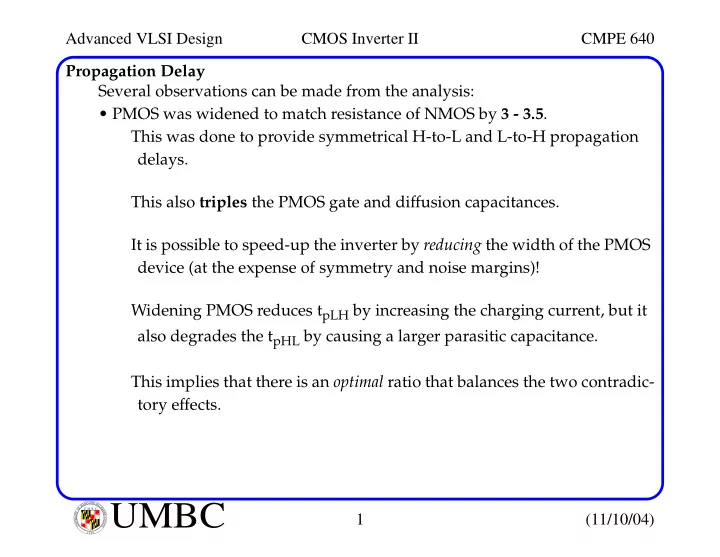
Advanced VLSI Design CMOS Inverter II CMPE 640 Propagation Delay Several observations can be made from the analysis: PMOS was widened to match resistance of NMOS by 3 - 3.5 . This was done to provide symmetrical H-to-L and L-to-H
Advanced VLSI Design CMOS Inverter II CMPE 640 Propagation Delay Several observations can be made from the analysis: • PMOS was widened to match resistance of NMOS by 3 - 3.5 . This was done to provide symmetrical H-to-L and L-to-H propagation delays. This also triples the PMOS gate and diffusion capacitances. It is possible to speed-up the inverter by reducing the width of the PMOS device (at the expense of symmetry and noise margins)! Widening PMOS reduces t pLH by increasing the charging current, but it also degrades the t pHL by causing a larger parasitic capacitance. This implies that there is an optimal ratio that balances the two contradic- tory effects. L A N R Y D UMBC A B M A L T F O U M B C I M Y O R T 1 (11/10/04) I E S R C E O V U I N N U T Y 1 6 9 6
Advanced VLSI Design CMOS Inverter II CMPE 640 Propagation Delay Consider two identically sized CMOS inverters. The load cap of the first gate is approximated by: ( ) ( ) C L C dp 1 C dn 1 C gp 2 C gn 2 C W = + + + + Now assume PMOS devices are made β times larger than NMOS. β C dn 1 β C gn 1 C dp 1 C gp 1 & = = ( β ) C dn 1 ( ) C L C gn 2 C W = 1 + + + Returning to: t pHL t pLH R eqp + t p 0.69 C L R eqn = - - - - - - - - - - - - - - - - - - - - - - - - - - - - - - - = + - - - - - - - - - - - - β 2 R eqp 0.69 ( ( β ) C dn 1 ( ) ) R eqn t p C gn 2 C W = - - - - - - - - - - 1 + + + + - - - - - - - - - - - - β 2 r ( ( β ) C dn 1 ( ) ) R eqn 1 t p C gn 2 C W = 0.345 1 + + + + - - - β L A N R Y D UMBC A B M A L T F O U M B C I M Y O R T 2 (11/10/04) I E S R C E O V U I N N U T Y 1 6 9 6
Advanced VLSI Design CMOS Inverter II CMPE 640 Propagation Delay r is equal to the resistance ratio of identically sized PMOS and NMOS transis- tors: R eqp /R eqn . The optimal value of β can be found by setting ∂ t p C W β opt r 1 = 0 = + - - - - - - - - - - - - - - - - - - - - - - - - - - - - - - - - ∂ β C dn 1 C gn 1 + When wiring capacitance is negligable, β opt equals the sqrt(r) , vs. r normally used in the non-cascaded case. If wiring cap dominates, larger values of β should be used. This analysis indicates that smaller device sizes (and smaller area) yield a faster design at the expense of symmetry and noise margins. Example in text gives β of 2.4 (=31 k Ω /13 k Ω ) for symmetrical response. β opt is then 1.6 -- SPICE sims gives optimal value of β = 1.9. L A N R Y D UMBC A B M A L T F O U M B C I M Y O R T 3 (11/10/04) I E S R C E O V U I N N U T Y 1 6 9 6
Advanced VLSI Design CMOS Inverter II CMPE 640 Sizing Inverters for Performance Assume a symmetrical inverter (rise and fall times of inverter are identical). Load capacitance can be divided into intrinsic or self-loading and extrinsic components: C L C int C ext = + Assuming R eq stands for the equivalent resistance of the gate, then propaga- tion delay is: ( ) t p 0.69 R eq C int C ext = + Intrinsic or unloaded delay C ext 0.69 R eq C int 1 = + - - - - - - - - - - - C int C ext t p 0 1 t p 0 0.69 R eq C int = + - - - - - - - - - - - = with C int So how does transistor sizing impact the performance of the gate? L A N R Y D UMBC A B M A L T F O U M B C I M Y O R T 4 (11/10/04) I E S R C E O V U I N N U T Y 1 6 9 6
Advanced VLSI Design CMOS Inverter II CMPE 640 Sizing Inverters for Performance C int consists of the diffusion and Miller caps, both of which are proportional to the width of the transistors. Let’s use a minimum sized inverter as a reference gate, then: R ref C int SC iref = R eq & = - - - - - - - - - - - S where S is the sizing factor . Re-writing previous expression: R ref C ext SC iref ( ) 1 t p - - - - - - - - - - - = 0.69 + - - - - - - - - - - - - - - - - S SC iref C ext 0.69 R ref C iref 1 = + - - - - - - - - - - - - - - - - SC iref L A N R Y D UMBC A B M A L T F O U M B C I M Y O R T 5 (11/10/04) I E S R C E O V U I N N U T Y 1 6 9 6
Advanced VLSI Design CMOS Inverter II CMPE 640 Sizing Inverters for Performance Conclusions: • Intrinsic delay of the inverter t p0 is independent of the sizing of the gate (determined by technology and layout only). When there is no load, the increase in drive of the gate is totally offset by increased cap. • Making S infinitely large yields the max performance, eliminates the impact of any external load and reduces the delay to the intrinsic one. Bear in mind that any size greater than (C ext /C int ) produces similar results while increasing the silicon area -- no win beyond this size. Bear in mind that although sizing up an inverter reduces its delay, it also increases its input capacitance. So the more relevant problem is determining the optimum size of a gate when embedded in a real environment. L A N R Y D UMBC A B M A L T F O U M B C I M Y O R T 6 (11/10/04) I E S R C E O V U I N N U T Y 1 6 9 6
Advanced VLSI Design CMOS Inverter II CMPE 640 Sizing Inverters for Performance Consider a chain of inverters as the first case. To determine input loading effect, we need to determine the relationship between the input gate capacitance , C g and the intrinsic output capacitance . Both are proportional to gate sizing, so the following is true: γ C g C int = The gamma factor γ is only a function of technology and is close to 1 for most processes. Substituting: C ext ( ⁄ γ ) t p t p 0 1 t p 0 1 f = + - - - - - - - - - - - = + γ C g This shows the delay of an inverter is only a function of the ratio between its external load cap and its input cap, and is called effective fan-out f . L A N R Y D UMBC A B M A L T F O U M B C I M Y O R T 7 (11/10/04) I E S R C E O V U I N N U T Y 1 6 9 6
Advanced VLSI Design CMOS Inverter II CMPE 640 Sizing a Chain of Inverters Goal is to minimize delay through the following inverter chain: In N 1 2 C L C g1 input cap of first inverter, min sized gate Some large load we need to drive Delay for j-th inverter stage (ignoring wire cap): C g j , + 1 ( f j γ ⁄ ) t p j t p 0 1 t p 0 1 = + - - - - - - - - - - - - - - - - - - - - = + , γ C g j , The total delay of the chain is then: N N C g j , ∑ ∑ + 1 t p j t p j t p 0 with C g, N+1 = C L = = 1 + - - - - - - - - - - - - - - - - - - - - , , γ C g j , j j = 1 = 1 And we need to solve for N-1 unknowns C g,2 , C g,3 , C g,N . L A N R Y D UMBC A B M A L T F O U M B C I M Y O R T 8 (11/10/04) I E S R C E O V U I N N U T Y 1 6 9 6
Advanced VLSI Design CMOS Inverter II CMPE 640 Sizing a Chain of Inverters Solution giving the optimal size of each inverter (that minimizes delay) is the geometric mean of each of the inverter’s neighbors: C g j C g j C g j = , , , – 1 + 1 So each inverter is sized up by the same factor f (and has the same delay). Given C g,1 and C L , the sizing factor is given as: N ⁄ f N C L C g 1 F = = , where F represents the overall effective fan-out of the circuit and equals C L /C g,1 . The minimum delay through the chain is: N ( ( ) γ ⁄ ) t p Nt p 0 1 F = + First component is intrinsic delay of the stages while second is effective fan-out of each stage. L A N R Y D UMBC A B M A L T F O U M B C I M Y O R T 9 (11/10/04) I E S R C E O V U I N N U T Y 1 6 9 6
Advanced VLSI Design CMOS Inverter II CMPE 640 Sizing a Chain of Inverters The relationship between t p and F is a strong function of the number of stages. The important question now is how to choose the number of stages so that the delay is minimized for a given value of F (C L /C g,1 ). If too many, intrinsic delay dominates, if too few, effective fan-out dominates. Differentiating and setting to zero yields: N ( ) F F N ln γ F or + – - - - - - - - - - - - - - - - - - - - - - - - - = 0 N ( γ ⁄ ) f e 1 + f = Under the condition that γ is 0 (self-loading is ignored, load cap only consists of the fan-out), the optimal number is: ( ) N F effective fan-out is set to f = e = 2.71828 = ln L A N R Y D UMBC A B M A L T F O U M B C I M Y O R T 10 (11/10/04) I E S R C E O V U I N N U T Y 1 6 9 6
Recommend
More recommend
Explore More Topics
Stay informed with curated content and fresh updates.


