UMBC A B M A L T F O U M B C I M Y O R T 1 - PowerPoint PPT Presentation
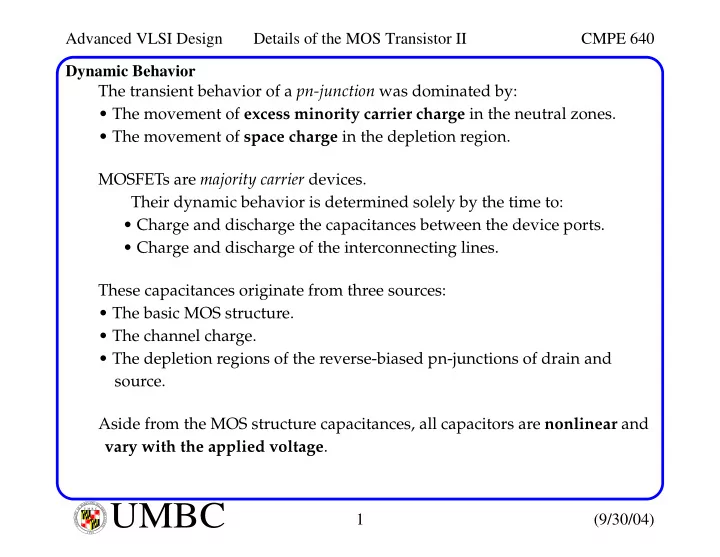
Advanced VLSI Design Details of the MOS Transistor II CMPE 640 Dynamic Behavior The transient behavior of a pn-junction was dominated by: The movement of excess minority carrier charge in the neutral zones. The movement of space charge in
Advanced VLSI Design Details of the MOS Transistor II CMPE 640 Dynamic Behavior The transient behavior of a pn-junction was dominated by: • The movement of excess minority carrier charge in the neutral zones. • The movement of space charge in the depletion region. MOSFETs are majority carrier devices. Their dynamic behavior is determined solely by the time to: • Charge and discharge the capacitances between the device ports. • Charge and discharge of the interconnecting lines. These capacitances originate from three sources: • The basic MOS structure. • The channel charge. • The depletion regions of the reverse-biased pn-junctions of drain and source. Aside from the MOS structure capacitances, all capacitors are nonlinear and vary with the applied voltage . L A N R Y D UMBC A B M A L T F O U M B C I M Y O R T 1 (9/30/04) I E S R C E O V U I N N U T Y 1 6 9 6
Advanced VLSI Design Details of the MOS Transistor II CMPE 640 Dynamic Behavior MOS Structure Capacitances: The gate of a MOS transistor is isolated from the channel by the gate oxide where: ε ox C ox = - - - - - - - - t ox For the I-V equations, it is useful to have C ox as large as possible, by keeping the oxide very thin. This capacitance is called gate capacitance and is given by: C g C ox WL = This gate capacitance can be decomposed into several parts: • One part contributes to the channel charge. • A second part is due to the topological structure of the transistor. Let’s consider the latter first. L A N R Y D UMBC A B M A L T F O U M B C I M Y O R T 2 (9/30/04) I E S R C E O V U I N N U T Y 1 6 9 6
Advanced VLSI Design Details of the MOS Transistor II CMPE 640 Dynamic Behavior MOS Structure Capacitances, Overlap: poly Poly t ox source drain W x d x d n+ n+ L eff n + n + L Lateral diffusion: source and drain diffusion extend under the oxide by an amount x d . The effective channel length (L eff ) is less than the drawn length L by 2*x d . This also gives rise to a linear, fixed capacitance called overlap capaci- tance . C gsO C gdO C ox x d W C O W = = = Since x d is technology dependent, it is usually combined with C ox . L A N R Y D UMBC A B M A L T F O U M B C I M Y O R T 3 (9/30/04) I E S R C E O V U I N N U T Y 1 6 9 6
Advanced VLSI Design Details of the MOS Transistor II CMPE 640 Dynamic Behavior Channel Charge: The gate-to-channel capacitance is composed of three components, C gs , C gd and C gb . Each of these is non-linear and dependent on the region of operation. Estimates or average values are often used: • Triode: C gb ~=0 since the inversion region shields the bulk electrode from the gate. • Saturation: C gb and C gd is ~= 0 since the channel is pinched off. C gb C gs C gd Operation Region Cutoff C ox WL eff 0 0 Triode C ox WL eff /2 C ox WL eff /2 0 Saturation (2/3)C ox WL eff 0 0 L A N R Y D UMBC A B M A L T F O U M B C I M Y O R T 4 (9/30/04) I E S R C E O V U I N N U T Y 1 6 9 6
Advanced VLSI Design Details of the MOS Transistor II CMPE 640 Dynamic Behavior Junction or Diffusion Capacitances: This component is caused by the reverse-biased source-bulk and drain- bulk pn-junctions . We determined that this capacitance is non-linear and decreases as reverse-bias is increased . sidewall W N D channel-stop + implant N A Bottom channel sidewall x j L S • Bottom-plate junction: Depletion region capacitance is: C bottom C j WL S = with a grading coefficient of m = 0.5 (for an abrupt junction) L A N R Y D UMBC A B M A L T F O U M B C I M Y O R T 5 (9/30/04) I E S R C E O V U I N N U T Y 1 6 9 6
Advanced VLSI Design Details of the MOS Transistor II CMPE 640 Dynamic Behavior MOS Structure Capacitances, Junction or Diffusion: • Side-wall junction: Formed by the source region with doping N D and the p + channel-stop + . implant with doping N A Since the channel-stop doping is usually higher than the substrate, this results in a higher unit capacitance: C ′ jsw x j W ( × ) C sw L S = + 2 with a grading coefficient of m = 1/3. Note that the channel side is not included in the calculation. x j is usually technology dependent and combined with C’ jsw as C jsw . Total junction (small-signal) capacitance is: × × C diff C bottom C sw C j AREA C jsw PERIMETER = + = + ( ) C diff C j L S W C jsw 2 L S W = + + As we’ve done before, we linearize these and use average cap. L A N R Y D UMBC A B M A L T F O U M B C I M Y O R T 6 (9/30/04) I E S R C E O V U I N N U T Y 1 6 9 6
Advanced VLSI Design Details of the MOS Transistor II CMPE 640 Dynamic Behavior Capacitive Device Model: The previous model can be summarized as: G C GS = C gs + C gsO C GS C GD C GD = C gd + C gdO D S C GB = C gb C SB C GB C DB C SB = C Sdiff C DB = C Ddiff B The dynamic performance of digital circuits is directly proportional to these capacitances. L A N R Y D UMBC A B M A L T F O U M B C I M Y O R T 7 (9/30/04) I E S R C E O V U I N N U T Y 1 6 9 6
Advanced VLSI Design Details of the MOS Transistor II CMPE 640 Dynamic Behavior Example: Given: 10 10 – × ⁄ C O F m t ox 6 nm = 3 = – F m 2 10 3 × ⁄ L 0.24 um C j 0 = = 2 10 10 – × ⁄ W 0.36 um C jsw 0 F m = = 2.75 L D L S 0.625 um = = Determine the zero-bias value of all relevant capacitances. Gate capacitance, C ox , per unit area is derived as: – f F um 10 2 × ⁄ 3.5 5.8 f F um 2 ε ox t ox ⁄ ⁄ C ox = = - - - - - - - - - - - - - - - - - - - - - - - - - - - - - - - - - - - - - - - - - - - - - = – 3 × 10 um 6 Total gate capacitance C g is: 5.8 f F um 2 × × ⁄ C g WLC ox 0.36 um 0.24 um 0.5 fF = = = Overlap capacitance is: C GSO C GDO WC O 0.108 fF = = = Total gate capacitance is: × C gtot C g C GSO 0.716 fF = + 2 = L A N R Y D UMBC A B M A L T F O U M B C I M Y O R T 8 (9/30/04) I E S R C E O V U I N N U T Y 1 6 9 6
Advanced VLSI Design Details of the MOS Transistor II CMPE 640 Dynamic Behavior Example (cont): Diffusion capacitance is the sum of bottom: 2 fF um 2 ⁄ × × C j 0 L D W 0.625 um 0.36 um 0.45 fF = = Plus side-wall (under zero-bias): – 1 ( ) × 10 ( × ) C jsw 0 2 L D W 0.625 um 0.36 um 0.44 fF + = 2.75 2 + = In this example, diffusion capacitance dominates gate capacitance (0.89 fF vs. 0.716 fF). Note that this is the worst case condition. Increasing reverse bias reduces diffusion capacitance (by about 50%). Also note that side-wall dominates diffusion. Advanced processes use + implant. SiO 2 to isolate devices (trench isolation) instead of N A Usually, diffusion is at most equal to gate, very often it is smaller. L A N R Y D UMBC A B M A L T F O U M B C I M Y O R T 9 (9/30/04) I E S R C E O V U I N N U T Y 1 6 9 6
Advanced VLSI Design Details of the MOS Transistor II CMPE 640 Source-Drain Resistance Scaling causes junctions to be shallower and contact openings to be smaller . This increases the parasitic resistance in series with the source and drain. Gate Drain G contact V GS,eff L D D S W R D R S Drain This resistance can be expressed as: R C L S D = Contact Resistance , R S D - R R C Sheet resistance 2 Ω ( 100 Ω ) R - - - - - - - - - - - = + , = – W L S,D = length of source/drain region. The series resistance degrades performance by decreasing drain current. Silicidation used -- low-resistivity material such as titanium or tungsten . L A N R Y D UMBC A B M A L T F O U M B C I M Y O R T 10 (9/30/04) I E S R C E O V U I N N U T Y 1 6 9 6
Advanced VLSI Design Details of the MOS Transistor II CMPE 640 Secondary Effects Long-channel devices : One-dimensional model discussed thus far. Assumed: • All current flows on the surface of the silicon. • Electric fields are oriented along that plane. Appropriate for manual analysis. Short-channel device : Ideal model does not hold well when device dimensions reach sub- micron range. The length of the channel becomes comparable to other device parameters such as the depth of the drain and source junctions. Two-dimensional model is needed. Computer simulation required. L A N R Y D UMBC A B M A L T F O U M B C I M Y O R T 11 (9/30/04) I E S R C E O V U I N N U T Y 1 6 9 6
Advanced VLSI Design Details of the MOS Transistor II CMPE 640 Secondary Effects Threshold variations: Ideal model assumed threshold voltage was only a function of technology parameters and applied body bias, V SB . With smaller dimensions, the V T0 becomes a function of L, W and V DS . For example, the expression for V T0 assumed that all depletion charge beneath the gate originates from the MOS field effects. We ignored the source and reverse-biased drain depletion regions. These depletion regions extend under the gate, which in turn reduces the threshold voltage necessary to cause strong inversion. V T V T Short-channel threshold Long-channel threshold Short-channel threshold L V DS Threshold as a function Drain-induced barrier lowering of length (for low V DS ) for small L. L A N R Y D UMBC A B M A L T F O U M B C I M Y O R T 12 (9/30/04) I E S R C E O V U I N N U T Y 1 6 9 6
Recommend
More recommend
Explore More Topics
Stay informed with curated content and fresh updates.


