UMBC A B M A L T F O U M B C I M Y O R T 1 - PowerPoint PPT Presentation
Digital Systems Clock Distribution II CMPE 650 Differential Distribution Differential clocks are more robust to noisy environments than single-ended clocks for 2 reasons: Signal swing is twice that of single-ended. Therefore, they can
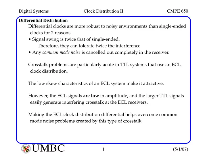
Digital Systems Clock Distribution II CMPE 650 Differential Distribution Differential clocks are more robust to noisy environments than single-ended clocks for 2 reasons: • Signal swing is twice that of single-ended. Therefore, they can tolerate twice the interference • Any common mode noise is cancelled out completely in the receiver. Crosstalk problems are particularly acute in TTL systems that use an ECL clock distribution. The low skew characteristics of an ECL system make it attractive. However, the ECL signals are low in amplitude, and the larger TTL signals easily generate interfering crosstalk at the ECL receivers. Making the ECL clock distribution differential helps overcome common mode noise problems created by this type of crosstalk. L A N R Y D UMBC A B M A L T F O U M B C I M Y O R T 1 (5/1/07) I E S R C E O V U I N N U T Y 1 6 9 6
Digital Systems Clock Distribution II CMPE 650 Differential Distribution Bear in mind that this strategy does not help with "single-sided" crosstalk, i.e., crosstalk created by one clock wire and a signal wire running too close to one another. Differential signaling helps a lot with communications between boards . The difference in the noise voltage on the GND planes of the two sys- tems cancel in the differential receiver. Clock Duty Cycle: The ideal duty cycle for a clock signal is 50%. The falling edge precisely bisects the signal changes in data wires. The average DC value of an ideal clock lies halfway between the HI and LO states. The property allows for the design of a simple feedback mechanism designed to keep the duty cycle fixed at 50%. L A N R Y D UMBC A B M A L T F O U M B C I M Y O R T 2 (5/1/07) I E S R C E O V U I N N U T Y 1 6 9 6
Digital Systems Clock Distribution II CMPE 650 Clock Signal Duty Cycle The asymmetric nature of rising/falling wfms of clock repeaters is the reason why clocks drift away (become unbalanced) form the 50% duty cycle. All gates have asymmetric response with regard to their rising and fall- ing edges. A pulse that propagates through a gate is either shortened ( pulse width compression ) or lengthened ( pulse width expansion ). As a chain of gates gets longer, the level of pulse width distortion adds. For example, assume the input pulse is positive-going and assume the delay of the rising edge exceeds the delay of the falling edge. The succession of positive pulses will become increasing shorter, and eventually disappear for long strings of buffers. L A N R Y D UMBC A B M A L T F O U M B C I M Y O R T 3 (5/1/07) I E S R C E O V U I N N U T Y 1 6 9 6
Digital Systems Clock Distribution II CMPE 650 Clock Signal Duty Cycle Two tricks can be used to solve this problem. • Invert the clock signal at every stage in an inverting chain . This converts rising edges to falling ones and cancels pulse width com- pression in adjacent stages, over that of a non-inverting chain. • Use an analog circuit that tracks the average DC value. 1K C 2 0.047 input threshold adjusted by C 2 OUT IN V BB V EE This only works with logic that has symmetric switching thresholds. L A N R Y D UMBC A B M A L T F O U M B C I M Y O R T 4 (5/1/07) I E S R C E O V U I N N U T Y 1 6 9 6
Digital Systems Clock Distribution II CMPE 650 Clock Signal Duty Cycle This circuit computes the average DC value and stores it on C 2. The value on C 2 adjusts the input switching threshold to achieve an output duty cycle closer to 50%. Canceling Parasitic Capacitance of Clock Repeaters Adding a device to the clock wire adds parasitic capacitance, which shifts the received clock phase on all devices on the line. This circuit can be used to combat the parasitic capacitance. Clock input C p L 1 V CC parasitic R 1 100K capacitance of circuit trace, R 2 C 1 100K connector and gate. L A N R Y D UMBC A B M A L T F O U M B C I M Y O R T 5 (5/1/07) I E S R C E O V U I N N U T Y 1 6 9 6
Digital Systems Clock Distribution II CMPE 650 Canceling Parasitic Capacitance of Clock Repeaters The inductor presents a negative reactance at the clock frequency and par- tially cancels the parasitic capacitance of the clk receiver circuit. This is called a matching network. Note the inductor-cancellation trick works only at the fundamental fre- quency , higher harmonics get no relief. Be sure to use a clk driver with slow rise and fall times. Such clks have lower harmonic content (more sinusoidal-like) and the neutralizing effect works better. The two resistors are optional. However, when used in a hot plugging environment, if they are absent, then a surge of current to charge C 1 will distort the clock signal. A properly designed hot plug card receives power before touching the clock bus, and therefore, the resistors, if present, provide the charging current. L A N R Y D UMBC A B M A L T F O U M B C I M Y O R T 6 (5/1/07) I E S R C E O V U I N N U T Y 1 6 9 6
Digital Systems Clock Distribution II CMPE 650 Canceling Parasitic Capacitance of Clock Repeaters Keeping C 1 small helps shorten the precharge time. The minimum value for C 1 is about 100 times C p. C 1 100 C p = 1 1 L 1 = - - - - - - - - - - - - - - - - - - - - - - - - + - - - - - - - - - - - - - - - - - - - - - - - - - ) 2 C 1 ) 2 C p ( 2 π f ( 2 π f With R 1 and R 2 present, the precharge time to bring C 1 within 1% of its final value, (HI+LO)/2, is given as: R 1 R 2 t pc - C 1 = 4.6 - - - - - - - - - - - - - - - - - - R 1 R 2 + Decoupling Clock Receivers from the Clock Bus Clock taps on the clk bus can seriously distort the clk wfm. Occurs when there are lots of taps, when the taps have large cap or when operating at high speed. L A N R Y D UMBC A B M A L T F O U M B C I M Y O R T 7 (5/1/07) I E S R C E O V U I N N U T Y 1 6 9 6
Digital Systems Clock Distribution II CMPE 650 Decoupling Clock Receivers from the Clock Bus One way to reduce the impact is to build a 3:1 attenuator at the input to each clock gate (receiver). This will require more voltage gain in each clk receiver. The attenuation network is inserted in series with clk receiver, at an imped- ance that is twice that of the receiver at the clock frequency. This effectively triples the apparent input impedance of the receiver. It also reduces the voltage to be interpreted by the receiver, but most gates have a lot of excess voltage gain. Differential receiver circuits are commonly used here, which have plenty of gain and a precisely controlled input-switching threshold. L A N R Y D UMBC A B M A L T F O U M B C I M Y O R T 8 (5/1/07) I E S R C E O V U I N N U T Y 1 6 9 6
Recommend
More recommend
Explore More Topics
Stay informed with curated content and fresh updates.


