UMBC A B M A L T F O U M B C I M Y O R T 1 - PowerPoint PPT Presentation
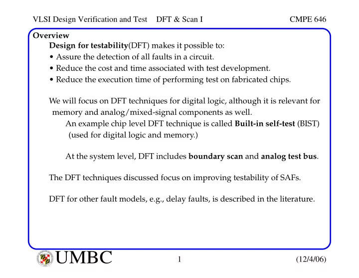
VLSI Design Verification and Test DFT & Scan I CMPE 646 Overview Design for testability (DFT) makes it possible to: Assure the detection of all faults in a circuit. Reduce the cost and time associated with test development.
VLSI Design Verification and Test DFT & Scan I CMPE 646 Overview Design for testability (DFT) makes it possible to: • Assure the detection of all faults in a circuit. • Reduce the cost and time associated with test development. • Reduce the execution time of performing test on fabricated chips. We will focus on DFT techniques for digital logic, although it is relevant for memory and analog/mixed-signal components as well. An example chip level DFT technique is called Built-in self-test (BIST) (used for digital logic and memory.) At the system level, DFT includes boundary scan and analog test bus . The DFT techniques discussed focus on improving testability of SAFs. DFT for other fault models, e.g., delay faults, is described in the literature. L A N R Y D UMBC A B M A L T F O U M B C I M Y O R T 1 (12/4/06) I E S R C E O V U I N N U T Y 1 6 9 6
VLSI Design Verification and Test DFT & Scan I CMPE 646 Ad-hoc DFT Two forms of DFT: ad-hoc and structured . Ad-hoc DFT relies on "good" design practices: • Avoid asynchronous logic feedbacks. Feedback can result in oscillation. ATPG are designed to work on acyclic combinational logic. • Make FFs initializable, i.e., provide clear and reset. • Avoid gates with a large fan-in. Large fan-in makes the inputs difficult to observe and the output diffi- cult to control. • Provide test control for difficult to control signals. For example, signals produced by a long counter require many clk cycles to control. This increases the length of the test sequence. L A N R Y D UMBC A B M A L T F O U M B C I M Y O R T 2 (12/4/06) I E S R C E O V U I N N U T Y 1 6 9 6
VLSI Design Verification and Test DFT & Scan I CMPE 646 Structured DFT Testability measures can be used to identify circuit areas that are difficult to test. Once identified, circuit is modified or test points are inserted. This type of ad-hoc strategy is difficult to use in large circuits: • Testability measures are approximations and don’t always work. • Good fault coverage is not guaranteed from ATPG even after circuit modi- fications and test point insertion is performed. Structured DFT involves adding extra logic and signals dedicated for test according to some procedure. The circuit has two modes, normal and test mode. The most commonly used structured methods are Scan and BIST. L A N R Y D UMBC A B M A L T F O U M B C I M Y O R T 3 (12/4/06) I E S R C E O V U I N N U T Y 1 6 9 6
VLSI Design Verification and Test DFT & Scan I CMPE 646 Scan Scan proposed in ’73 by Williams and Angell. Main idea is to obtain control and observability for FFs. It reduces sequential TPG to combinational TPG. With Scan, a synchronous sequential circuit works in two modes. Normal mode and test mode: PIs POs PIs POs Combo logic Combo logic FFs FFs Scan-in Scan-out In test mode , all FFs are configured as a shift register, with Scan-in and Scan-out routed to a (possibly dedicated) PI and PO. L A N R Y D UMBC A B M A L T F O U M B C I M Y O R T 4 (12/4/06) I E S R C E O V U I N N U T Y 1 6 9 6
VLSI Design Verification and Test DFT & Scan I CMPE 646 Scan Once initialized, normal mode is used to apply a pattern to the PIs, and the results are latched in the FFs. The circuit is put in test mode again and the results scanned out. PIs POs PIs POs Combo logic Combo logic Scan FFs Variations FFs FFs FFs Partial Scan Multiple Scan chains Note that scan is usually inserted after the circuit is verified to be functionally correct. L A N R Y D UMBC A B M A L T F O U M B C I M Y O R T 5 (12/4/06) I E S R C E O V U I N N U T Y 1 6 9 6
VLSI Design Verification and Test DFT & Scan I CMPE 646 Scan-Path Design Any sequential circuit may be modeled as: X 1 Z 1 X 2 Next state and output Z 2 combinational logic X K Z N D Q D Q D Q FF 1 FF 2 FF 3 Clk X 1 Z 1 X 2 Next state and output Z 2 combinational logic (Note, latches cannot be used here) X K Z N 0 0 0 0 D Q D Q D Q 1 1 1 1 SO FF 1 FF 2 FF 3 SI Clk Scan-Enable (SE) L A N R Y D UMBC A B M A L T F O U M B C I M Y O R T 6 (12/4/06) I E S R C E O V U I N N U T Y 1 6 9 6
VLSI Design Verification and Test DFT & Scan I CMPE 646 Scan Design Rules A designer needs to observe four rules during functional design: • Only D-type master-slave FFs should be used. No JK , toggle FFs or other forms of asynchronous logic. • At least on PI must be available for test. As shown in previous circuit, the Scan-in and Scan-out pins can be mul- tiplexed (only one additional MUX is needed at Scan-out). Therefore, the only required extra pin is Scan-Enable, SE (or Test Control, TC). • All FFs must be controlled from PIs. Simple circuit transformations can be used to change FFs whose Clk is "gated" by an internal logic signal. • Clocks must not feed data inputs of the FFs. A race condition can result in normal mode otherwise. This is generally considered good design practice anyway. L A N R Y D UMBC A B M A L T F O U M B C I M Y O R T 7 (12/4/06) I E S R C E O V U I N N U T Y 1 6 9 6
VLSI Design Verification and Test DFT & Scan I CMPE 646 Storage Cells for Scan Designs Common characteristics of all designs: • A normal input and a scan input . The appropriate input can be selected using a multiplexer or by a two- clock system. • A storage cell . The cell can be implemented using an edge-triggered FF, a master-slave FF or level-sensitive latches controlled by clocks having >=2 phases. We’ll focus only on D-FFs of the master-slave variety. D Latch Q D Q φ Q Q φ D-Latch L A N R Y D UMBC A B M A L T F O U M B C I M Y O R T 8 (12/4/06) I E S R C E O V U I N N U T Y 1 6 9 6
VLSI Design Verification and Test DFT & Scan I CMPE 646 Storage Cells for Scan Designs An implementation using two-port master-slave FF with a MUX . 2-to-1 MUX D L 1 L 2 Q 1 Q 2 Q Q D D SI φ φ Sel Q Q φ A two-port clocked FF implementation. D φ 1 L 1 L 2 Q 1 Q 2 Q Q D D SI φ 2 φ φ Q Q L A N R Y D UMBC A B M A L T F O U M B C I M Y O R T 9 (12/4/06) I E S R C E O V U I N N U T Y 1 6 9 6
VLSI Design Verification and Test DFT & Scan I CMPE 646 Storage Cells for Scan Designs To ensure race-free operation, use a 2-phase nonoverlapping clk. D L 1 L 2 Q 1 Q 2 Q Q D D SI φ φ Sel Q Q φ 1 Not a FF, since two φ 2 clocks are used. In order to avoid performance degradation introduced by the MUX. Q 1 D L 2 (SO) Q 2 φ 1 SI L 1 φ 2 NAND version of LSSD φ 3 L A N R Y D UMBC A B M A L T F O U M B C I M Y O R T 10 (12/4/06) I E S R C E O V U I N N U T Y 1 6 9 6
VLSI Design Verification and Test DFT & Scan I CMPE 646 Storage Cells for Scan Designs In LSSD, clocks φ 1 and φ 2 can be NORed together to drive L 2 , replacing φ 3 . Q 1 D L 2 (SO) Q 2 φ 1 SI L 1 φ 2 Note that in the 3-clock scheme, in order to prevent hazards, φ 1 and φ 3 and well as φ 2 and φ 3 MUST be non-overlapping. φ 1 t φ 1 φ 3 t φ 3 L A N R Y D UMBC A B M A L T F O U M B C I M Y O R T 11 (12/4/06) I E S R C E O V U I N N U T Y 1 6 9 6
VLSI Design Verification and Test DFT & Scan I CMPE 646 Tests for Scan Circuits Two phases: • Shift test Set TC = 0, and shift toggle sequence 00110011... using Clk. The length is n sff + 4, where n sff are the number of scan flops. This sequence produces all 4 transitions, 0->0, 0->1, 1->1 and 1->0, catches all/most SA faults. The Shift test can be used in either single-clock or two-clock designs. A Flush test is also possible in two-clock designs: φ 1 (Master Clk) is held low while φ 2 and φ 3 are held high. This creates a continuous path between SI and SO for application of 0 and 1. • Combinational logic test This phase allows the combination logic circuit to be tested for SA faults. An ATPG algorithm is used where outputs of Scan FFs are treated as pseudo-PIs (completely controllable) and inputs are treated as pseudo- POs. L A N R Y D UMBC A B M A L T F O U M B C I M Y O R T 12 (12/4/06) I E S R C E O V U I N N U T Y 1 6 9 6
VLSI Design Verification and Test DFT & Scan I CMPE 646 Tests for Scan Circuits Each vector contains two parts: i x and s x represent PIs and pseudo-PIs (state variables), o x and n x represent POs and pseudo-POs (next state variables). Seq 1 Seq 2 Seq 3 Don’t Don’t Don’t Don’t PIs 9 scan vectors i 1 i 2 i 3 cares cares cares cares 1 normal vector s 1 s 2 s 3 Scanin TC 000000000 1 000000000 1 000000000 1 000000000 On 10th vector TC is set to 1. 39 Clks are o 1 o 2 o 3 needed for these n 1 n 2 n 3 Scanout 3 vectors. The vectors are converted as shown above. Don’t care bits can be filled randomly or with a specific sequence. Faults at POs under 1st vector are detected after 10th Clk. However, faults captured in FFs for this vector are detected on 11th through 19th Clk, during scanin of 2nd vector. L A N R Y D UMBC A B M A L T F O U M B C I M Y O R T 13 (12/4/06) I E S R C E O V U I N N U T Y 1 6 9 6
Recommend
More recommend
Explore More Topics
Stay informed with curated content and fresh updates.

