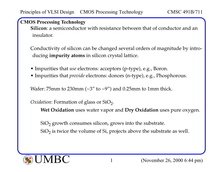

Principles of VLSI Design CMOS Processing Technology CMSC 491B/711 CMOS Processing Technology Silicon : a semiconductor with resistance between that of conductor and an insulator. Conductivity of silicon can be changed several orders of magnitude by intro- ducing impurity atoms in silicon crystal lattice. • Impurities that use electrons: acceptors (p-type), e.g., Boron. • Impurities that provide electrons: donors (n-type), e.g., Phosphorous. Wafer: 75mm to 230mm (~3” to ~9”) and 0.25mm to 1mm thick. Oxidation : Formation of glass or SiO 2 . Wet Oxidation uses water vapor and Dry Oxidation uses pure oxygen. SiO 2 growth consumes silicon, grows into the substrate. SiO 2 is twice the volume of Si, projects above the substrate as well. L A N R Y D UMBC A B M A L F T U M B C I O M Y O T R 1 (November 26, 2000 6:44 pm) I E S R C E O V U I N N U T Y 1 6 9 6
Principles of VLSI Design CMOS Processing Technology CMSC 491B/711 CMOS Processing Technology Epitaxy, Ion-Implantation and Deposition/Diffusion: Ways of introducing impurities into pure silicon. • Epitaxy : Single-crystal film grown on silicon surface. • Deposition : Evaporate dopant material onto surface, high temps drive impurities into silicon bulk (diffusion). • Ion implantation : Highly energized donor and acceptor atom driven into the silicon. How much dopant that is introduced is controlled by energy and amount of time. Where it is introduced is controlled by masks (thin films of special material). Mask materials include: photoresist polysilicon silicon dioxide (SiO 2 ) silicon nitride (SiN) L A N R Y D UMBC A B M A L F T U M B C I O M Y O T R 2 (November 26, 2000 6:44 pm) I E S R C E O V U I N N U T Y 1 6 9 6
Principles of VLSI Design CMOS Processing Technology CMSC 491B/711 CMOS Processing Technology Selective diffusion: Masks act as a barrier to prevent impurities from diffus- ing. Process involves: • Patterning windows in the mask on the die surface. • Introducing impurities in exposed regions. • Removing the mask. For example, to cut windows into the glass after oxidation step: Acid resistant coating (photoresist) spread evenly on surface. Photoresist SiO 2 (Glass) Silicon Wafer L A N R Y D UMBC A B M A L F T U M B C I O M Y O T R 3 (November 26, 2000 6:44 pm) I E S R C E O V U I N N U T Y 1 6 9 6
Principles of VLSI Design CMOS Processing Technology CMSC 491B/711 CMOS Processing Technology Polymerized in areas exposed by UV light. UV light Mask Mask Photoresist SiO 2 Silicon Wafer Mask controls region exposed. L A N R Y D UMBC A B M A L F T U M B C I O M Y O T R 4 (November 26, 2000 6:44 pm) I E S R C E O V U I N N U T Y 1 6 9 6
Principles of VLSI Design CMOS Processing Technology CMSC 491B/711 CMOS Processing Technology Organic solvent removes polymerized areas. Photoresist SiO 2 Silicon Wafer Windows are etched using an acid and the photoresist is removed. Photoresist SiO 2 Silicon Wafer SiO 2 Photoresist removed Silicon Wafer L A N R Y D UMBC A B M A L F T U M B C I O M Y O T R 5 (November 26, 2000 6:44 pm) I E S R C E O V U I N N U T Y 1 6 9 6
Principles of VLSI Design CMOS Processing Technology CMSC 491B/711 CMOS Processing Technology Positive resist: Exposed photoresist removed. Negative resist: Unexposed photoresist removed. UV light defraction and alignment tolerances limit line widths to ~0.8microns. Electron beam lithography : Reduces line width limits to 0.5microns. Adv: • No intermediate hardware images such as masks. • Changes to patterns can be implemented immediately. Disadv: • Cost of equipment is high. • Requires large amount of time to process each wafer. L A N R Y D UMBC A B M A L F T U M B C I O M Y O T R 6 (November 26, 2000 6:44 pm) I E S R C E O V U I N N U T Y 1 6 9 6
Principles of VLSI Design CMOS Processing Technology CMSC 491B/711 CMOS Processing Technology Polysilicon: A polycrystalline (not a single crystal) form of silicon. Used as: • Interconnection material. • Gate electrodes. • *** A mask to allow precise definition of source and drain ***. Undoped poly has a very high resistance. Poly and the source/drain regions are usually doped at the same time. Silicon Gate Process: Oxidation and etching of the active region: Active region SiO 2 - Field Oxide (isolates active regions from other active regions) p-substrate L A N R Y D UMBC A B M A L F T U M B C I O M Y O T R 7 (November 26, 2000 6:44 pm) I E S R C E O V U I N N U T Y 1 6 9 6
Principles of VLSI Design CMOS Processing Technology CMSC 491B/711 CMOS Processing Technology Thin Oxide grown: Thinox (10 -> 30nm) Field Oxide p-substrate Polysilicon deposited and etched: Poly Thinox Field Oxide p-substrate L A N R Y D UMBC A B M A L F T U M B C I O M Y O T R 8 (November 26, 2000 6:44 pm) I E S R C E O V U I N N U T Y 1 6 9 6
Principles of VLSI Design CMOS Processing Technology CMSC 491B/711 CMOS Processing Technology Etching of thinox and dopant Ion-Implantation or Deposition/Diffusion: *** Self-aligned source Field Oxide and drain *** do NOT gate extend under n+ n+ the gate. p-substrate SiO 2 and contact cuts. SiO 2 Contact cuts gate n+ n+ p-substrate L A N R Y D UMBC A B M A L F T U M B C I O M Y O T R 9 (November 26, 2000 6:44 pm) I E S R C E O V U I N N U T Y 1 6 9 6
Principles of VLSI Design CMOS Processing Technology CMSC 491B/711 CMOS Processing Technology Aluminum evaporated and etched: Aluminum contacts n+ n+ p-substrate L A N R Y D UMBC A B M A L F T U M B C I O M Y O T R 10 (November 26, 2000 6:44 pm) I E S R C E O V U I N N U T Y 1 6 9 6
Principles of VLSI Design CMOS Processing Technology CMSC 491B/711 CMOS Processing Technology Parasitic MOS transistor: Poly or m etal runner n+ n+ n+ n+ p-substrate U nexpected n-channel Field device transistor Field device Countermeasures: Make the threshold voltage of field device high by: • Making the field oxide thick. • Introducing a “channel-stop” diffusion (higher impurity concentration). L A N R Y D UMBC A B M A L F T U M B C I O M Y O T R 11 (November 26, 2000 6:44 pm) I E S R C E O V U I N N U T Y 1 6 9 6
Principles of VLSI Design CMOS Processing Technology CMSC 491B/711 CMOS Processing Technology Four main CMOS technologies: • n-well process • p-well process • twin-tub process • silicon on insulator Major process steps of n-well process: • n-well mask used to create n-well or n-tub via ion-implantation or deposi- tion/diffusion. n-w ell region for p-transistors n-w ell lightly doped p-substrate L A N R Y D UMBC A B M A L F T U M B C I O M Y O T R 12 (November 26, 2000 6:44 pm) I E S R C E O V U I N N U T Y 1 6 9 6
Principles of VLSI Design CMOS Processing Technology CMSC 491B/711 CMOS Processing Technology • active mask defines areas where transistors are fabricated. Silicon N itride (SiN ) Thinox n-w ell lightly doped p-substrate • p-well mask used to produce channel-stop (p + diffusion), field oxide grown. (Complement of n-well mask) Field oxide C hannel stop n-w ell lightly doped p-substrate L A N R Y D UMBC A B M A L F T U M B C I O M Y O T R 13 (November 26, 2000 6:44 pm) I E S R C E O V U I N N U T Y 1 6 9 6
Principles of VLSI Design CMOS Processing Technology CMSC 491B/711 CMOS Processing Technology • poly mask used to etch poly patterns. Poly n-w ell lightly doped p-substrate • n-plus mask ( select mask ) used to indicate those thin-oxide areas and poly that are to implanted n + . + diffusion n ic contacts O hm areas are also doped in n-w ells n-w ell for w ell plugs lightly doped p-substrate L A N R Y D UMBC A B M A L F T U M B C I O M Y O T R 14 (November 26, 2000 6:44 pm) I E S R C E O V U I N N U T Y 1 6 9 6
Principles of VLSI Design CMOS Processing Technology CMSC 491B/711 CMOS Processing Technology • p-plus mask used to indicate those thin-oxide areas and poly that are to implanted p + . ic contacts O hm areas are also doped in p-substrate for w ell plugs n-w ell lightly doped + diffusion p p-substrate • Surface is covered with SiO 2 and contact cuts made. C ontact SiO to poly cuts 2 to diffusion n-w ell lightly doped p-substrate L A N R Y D UMBC A B M A L F T U M B C I O M Y O T R 15 (November 26, 2000 6:44 pm) I E S R C E O V U I N N U T Y 1 6 9 6
Principles of VLSI Design CMOS Processing Technology CMSC 491B/711 CMOS Processing Technology • Metallization applied and etched using metal mask . A lum inum n-w ell lightly doped p-substrate • The wafer is then passivated and opening to bond pads are etched. L A N R Y D UMBC A B M A L F T U M B C I O M Y O T R 16 (November 26, 2000 6:44 pm) I E S R C E O V U I N N U T Y 1 6 9 6
Recommend
More recommend