UMBC A B M A L T F O U M B C I M Y O R T 1 - PowerPoint PPT Presentation
Programmable Logic Devices Verilog Introduction CMPE 415 EDA Electronic design automation (EDA) is the practice of using computer-based software systems to design VLSI circuits. Many tools exist within EDA -- we focus here on the hardware
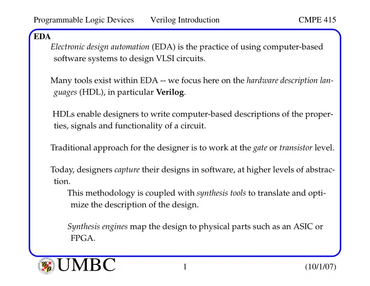
Programmable Logic Devices Verilog Introduction CMPE 415 EDA Electronic design automation (EDA) is the practice of using computer-based software systems to design VLSI circuits. Many tools exist within EDA -- we focus here on the hardware description lan- guages (HDL), in particular Verilog . HDLs enable designers to write computer-based descriptions of the proper- ties, signals and functionality of a circuit. Traditional approach for the designer is to work at the gate or transistor level. Today, designers capture their designs in software, at higher levels of abstrac- tion. This methodology is coupled with synthesis tools to translate and opti- mize the description of the design. Synthesis engines map the design to physical parts such as an ASIC or FPGA. L A N R Y D UMBC A B M A L T F O U M B C I M Y O R T 1 (10/1/07) I E S R C E O V U I N N U T Y 1 6 9 6
Programmable Logic Devices Verilog Introduction CMPE 415 EDA Despite the powerful features available in such an approach, HDLs have not been widely accepted because: • Many designs are of a size and complexity that allow schematic entry to be used successfully. • Many engineers lack a working familiarity with HDLs. Design flow Design specifications summarize the functional behavior , timing require- ments , and other relevant attributes including speed , power and area . Design entry is the process of encapsulating a representation of the design, i.e., schematic, state transition diagrams, HDL, etc. Each step in the design flow either: • Creates a database supporting the design flow • Verifies that the design meets specific criteria L A N R Y D UMBC A B M A L T F O U M B C I M Y O R T 2 (10/1/07) I E S R C E O V U I N N U T Y 1 6 9 6
Programmable Logic Devices Verilog Introduction CMPE 415 Design Flow A design flow starts with design entry and ends with photomasks or a pro- gramming file (for FPGAs). A successful design might require multiple, iterative passes through all or part of this flow. First design flow Second design flow Create gate-level desc. Write Verilog (consider testability) (consider testability) Verify/Simulate Verify/Simulate (generate test patterns) Verify timing Synthesize/optimize gate-level netlist Create masks DRC/extract parasitics L A N R Y D UMBC A B M A L T F O U M B C I M Y O R T 3 (10/1/07) I E S R C E O V U I N N U T Y 1 6 9 6
Programmable Logic Devices Verilog Introduction CMPE 415 Design Flow There are several physical realizations of the design in hardware. Each offers trade-offs with respect to time-to-market, cost, and performance. full-custom to amortize, time to Market volume std. cells prototype FPGAs, gate arrays VLSI course PLDs This course NRE cost, process complexity, density, speed, complexity L A N R Y D UMBC A B M A L T F O U M B C I M Y O R T 4 (10/1/07) I E S R C E O V U I N N U T Y 1 6 9 6
Programmable Logic Devices Verilog Introduction CMPE 415 Design Entry As indicated, design entry encapsulates a description of the design in a data- base that serves subsequent steps in the design fl ow . Schematics and HDLs are the two commonly used modes of entry. Schematic entry focuses on the structural detail of the design. Advantages: Familiarity of the designer with this visual format Disadv: Supports only a low to moderate level of circuit complexity. Almost all CAD tools support this mode of design entry, many with fancy graphical interfaces and verification tools. Divide and conquer through hierarchical decomposition is extensively used. a sum b sum a c_out b c_out Symbol Schematic L A N R Y D UMBC A B M A L T F O U M B C I M Y O R T 5 (10/1/07) I E S R C E O V U I N N U T Y 1 6 9 6
Programmable Logic Devices Verilog Introduction CMPE 415 Design Entry A HDL is a programming language with special constructs and semantics to model , represent , and simulate the function and timing of the hardware. Variables are used to represent electrical signals. Their semantics include both a value and time . This allows the temporal relationship of the signals to be described, generated and manipulated. Tools exist that convert the HDL text to schematic automatically. HDLs allow the designer to describe the design as a structural entity (such as that required by schematic). HDLs also allow the designer to describe the design as a behavioral entity , using procedural code. This decouples the description of the design from actual physical hard- ware. L A N R Y D UMBC A B M A L T F O U M B C I M Y O R T 6 (10/1/07) I E S R C E O V U I N N U T Y 1 6 9 6
Programmable Logic Devices Verilog Introduction CMPE 415 Structural Verilog The Verilog HDL counterpart of the schematic shown earlier: Module Ports Module Name module half_adder(sum, c_out, a, b); input a, b; output sum,c_out; Declaration of Port Modes wire c_out_bar; Declaration of Internal Signal xor (sum, a, b); nand (c_out_bar, a, b); Instantiation of Primitive Gates not (c_out, c_out_bar); endmodule Module Ports can be inout for bidirectional signals Gates are instantiated in the body of the module. IMPORTANT: The order of the statements within the module is inconse- quential -- signal values and assignments are functions of time! In programming languages such as C, order does matter. L A N R Y D UMBC A B M A L T F O U M B C I M Y O R T 7 (10/1/07) I E S R C E O V U I N N U T Y 1 6 9 6
Programmable Logic Devices Verilog Introduction CMPE 415 Behavioral Verilog As indicated, Verilog also allows behavioral descriptions of designs: module flip_flop(q, data_in, clk, rst); input data_in, clk, rst; output q; Declares q to be a register value , reg q; i.e., it retains its value once always @( posedge clk) it is assigned between clk edges. begin reg is an abstract memory variable if (rst == 1) q = 0; else q = data_in; end endmodule Here, execution halts at the always statement until clk has a rising edge. When this occurs, the body executes, which assigns q the value data_in unless rst is asserted. Once executed, execution is halted once again at the always statement until the next event ( clk has a rising edge) occurs. L A N R Y D UMBC A B M A L T F O U M B C I M Y O R T 8 (10/1/07) I E S R C E O V U I N N U T Y 1 6 9 6
Programmable Logic Devices Verilog Introduction CMPE 415 Behavioral Verilog The previous code is event-controlled . The event control statement ( always @... ) defines the sensitivity of the behav- ioral model to external signals. IMPORTANT: The stmts within the process block execute sequentially , just like they do within C (subject to any timing control expressions). Within Verilog, there are 3 types of timing controls: • Event control • Delay control • The wait statement The first 2 are intuitive, event control suspends execution until an event occurs, while delay control suspends execution for a specified time. The wait statement suspends execution until a condition is satisfied (more on this later). L A N R Y D UMBC A B M A L T F O U M B C I M Y O R T 9 (10/1/07) I E S R C E O V U I N N U T Y 1 6 9 6
Programmable Logic Devices Verilog Introduction CMPE 415 Behavioral Verilog A more complex behavioral model: module 4bit_RTL_adder(a, b, c_in, sum, c_out); output [3:0] sum; output c_out; Concatenation operator input [3:0] a, b; input c_in; assign {c_out, sum} = a + b + c_in; endmodule Sum operator The assign statement describes a behavior (addition) that requires several gates in actual hardware. The keyword assign and the ’+’ operator provide a shortcut , i.e., they describe the behavior of the circuit without a physical representation. The continuous assignment stmt describes implicit combinational logic. This style of Verilog is referred to as register transfer level ( RTL ) or data flow because it represents operations on a data path using operators. L A N R Y D UMBC A B M A L T F O U M B C I M Y O R T 10 (10/1/07) I E S R C E O V U I N N U T Y 1 6 9 6
Recommend
More recommend
Explore More Topics
Stay informed with curated content and fresh updates.

