UMBC A B M A L T F O U M B C I M Y O R T 1 - PowerPoint PPT Presentation
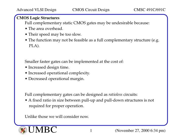
Advanced VLSI Design CMOS Circuit Design CMSC 491C/691C CMOS Logic Structures Full complementary static CMOS gates may be undesirable because: The area overhead. Their speed may be too slow. The function may not be feasible as a
Advanced VLSI Design CMOS Circuit Design CMSC 491C/691C CMOS Logic Structures Full complementary static CMOS gates may be undesirable because: • The area overhead. • Their speed may be too slow. • The function may not be feasible as a full complementary structure (e.g. PLA). Smaller faster gates can be implemented at the cost of: • Increased design time. • Increased operational complexity. • Decreased operational margin. Full complementary gates can be designed as ratioless circuits: • A fixed ratio in size between pull-up and pull-down structures is not required for proper operation. Unlike those we will consider now. L A N R Y D UMBC A B M A L T F O U M B C I M Y O R T 1 (November 27, 2000 6:34 pm) I E S R C E O V U I N N U T Y 1 6 9 6
Advanced VLSI Design CMOS Circuit Design CMSC 491C/691C CMOS Logic Structures Pseudo-nMOS logic Advantages: Capacitive load on inputs is only one gate unit. Z = A.(B+C)+(D.E) Density advantage over A full complementary CMOS. B Main problem: Static power dissipation C D Gain of the pull-up has to be decreased to provide adequate noise margins (when minimum E sized transistors are used). Slows rise time. Gain ratio of n-driver transistors to p-transistor load (beta driver /beta load ), is important to ensure correct operation. Accomplished by ratioing the n and p transistor sizes. L A N R Y D UMBC A B M A L T F O U M B C I M Y O R T 2 (November 27, 2000 6:34 pm) I E S R C E O V U I N N U T Y 1 6 9 6
Advanced VLSI Design CMOS Circuit Design CMSC 491C/691C CMOS Logic Structures Dynamic CMOS Logic Simple single phase dynamic CMOS: Precharge phase: Clk = 0 Evaluate phase: Clk = 1 z Input capacitance: Same as that of pseudo-nMOS. n-logic inputs Problem: block Inputs can only change during the precharge phase. If they change during evaluate, charge redistribution can clk corrupt output voltage. Pull-up time improved by virtue of the active switch (p-transistor can be much larger). Pull-down time increased due to the ground switch. L A N R Y D UMBC A B M A L T F O U M B C I M Y O R T 3 (November 27, 2000 6:34 pm) I E S R C E O V U I N N U T Y 1 6 9 6
Advanced VLSI Design CMOS Circuit Design CMSC 491C/691C CMOS Logic Structures Dynamic CMOS Logic Other inputs z z n-logic n-logic inputs block block clk What is wrong with cascading these structures? (Hint: Consider the delay in the discharge of the left-most n-logic block at the start of the evaluate phase). L A N R Y D UMBC A B M A L T F O U M B C I M Y O R T 4 (November 27, 2000 6:34 pm) I E S R C E O V U I N N U T Y 1 6 9 6
Advanced VLSI Design CMOS Circuit Design CMSC 491C/691C CMOS Logic Structures CMOS Domino Logic: Added a static Simple mod of Dynamic logic: CMOS inverter evaluate precharge z Next domino stage. A Only non-inverting forms of logic possible. B C Precharge phase: Output of buffer, z, is zero. D Evaluate phase: Output, z, E conditionally goes high. Dynamic circuit as shown: Can be made static or latching with Clk the addition of a (weak) p and feedback. These structures can be cascaded. In a cascaded set of logic blocks, each stage evaluates and causes the next stage to evaluate (in the same way a line of dominos fall). L A N R Y D UMBC A B M A L T F O U M B C I M Y O R T 5 (November 27, 2000 6:34 pm) I E S R C E O V U I N N U T Y 1 6 9 6
Advanced VLSI Design CMOS Circuit Design CMSC 491C/691C CMOS Logic Structures Pass-Transistor Logic: Control variables A A B B A (Values from P 1 registers). P 1 P 2 A F(A,B) P 3 Boolean Function Pass variables Unit P 4 (Set by opcode). P 4 P 3 P 2 P 1 Operation AND(A,B) 0 0 0 1 0 1 1 0 XOR(A,B) NOR(A,B) 1 0 0 0 L A N R Y D UMBC A B M A L T F O U M B C I M Y O R T 6 (November 27, 2000 6:34 pm) I E S R C E O V U I N N U T Y 1 6 9 6
Advanced VLSI Design CMOS Circuit Design CMSC 491C/691C CMOS Logic Structures Other forms of CMOS logic include: BiCMOS Logic Clocked CMOS Logic (C 2 MOS). NP Domino Logic (Zipper CMOS). Cascade Voltage Switch Logic (CVSL). Source Follower Pull-up Logic (SFPL). (See Weste and Eshraghian for details.) Where should one use what gate? Complementary: Best option for most cases. Safe, fast, no DC power. Pseudo-nMOS: Large fan-in NOR gates, i.e. PLAs, ROMs. DC power. Transmission gate: Speed advantage, good for complex boolean functions. CMOS domino logic: Low-power, high speed. Requires simulation! L A N R Y D UMBC A B M A L T F O U M B C I M Y O R T 7 (November 27, 2000 6:34 pm) I E S R C E O V U I N N U T Y 1 6 9 6
Advanced VLSI Design CMOS Circuit Design CMSC 491C/691C Clocked Systems Majority of VLSI systems are Finite State machines and Pipelined machines: Inputs Outputs Combinational Logic Current Next State State Q D Bits Bits clk(s) No feedback Feedback FSM outputs inputs D Q D Q D Q Logic Logic clk Pipelined System L A N R Y D UMBC A B M A L T F O U M B C I M Y O R T 8 (November 27, 2000 6:34 pm) I E S R C E O V U I N N U T Y 1 6 9 6
Advanced VLSI Design CMOS Circuit Design CMSC 491C/691C Clock Strategy One of the most important decisions made at the start of a design is the selec- tion of a clocking strategy. It effects: How many transistors are used per storage element. How many clock signals need to be routed throughout the chip. Topics: Latch, Master-Slave Flip-flop and Edge-Triggered Flip-flop designs. Setup and Hold time and clock race conditions. CMOS Static and Dynamic Flip-flops. Single phase clocking, clock skew/slew. Two-phase clocking techniques. Clock generation techniques. L A N R Y D UMBC A B M A L T F O U M B C I M Y O R T 9 (November 27, 2000 6:34 pm) I E S R C E O V U I N N U T Y 1 6 9 6
Advanced VLSI Design CMOS Circuit Design CMSC 491C/691C Latches and Flip-flops R Q S R Q Q Positive 0 0 Q Q NOR logic version 0 1 0 1 1 0 1 0 Q S 1 1 0 0 The length of the trigger pulse Note that this mode is forbidden Set-Reset since the constraint Q and Q applied to S or R has to larger than Flip-fl op are not complementary. Also, the loop delay of the cross-coupled the return to 00/11 leaves the FF pair. in an unpredictable state. S R Q Q S Q 0 0 1 1 NAND 0 1 1 0 Negative version logic 1 0 0 1 Q Q Q 1 1 R L A N R Y D UMBC A B M A L T F O U M B C I M Y O R T 10 (November 27, 2000 6:34 pm) I E S R C E O V U I N N U T Y 1 6 9 6
Advanced VLSI Design CMOS Circuit Design CMSC 491C/691C Latches and Flip-flops The ambiguity of having a non-allowed mode caused by trigger pulses going active simultaneously can be avoided by adding two feedback lines: Q n+1 J n K n J S Q 0 0 Q n 0 1 0 φ 1 0 1 Q n 1 1 Q K R Note if both J and K are high, and clock pulses, the output is complemented. However, doing so enables the other input and the FF oscillates . This places some stringent constraints on the clock pulse width (e.g. < than the propagation delay through the FF). Synchronous circuit: Changes in the output logic states of all FFs in a design are synchronized with the clock signal, phi. L A N R Y D UMBC A B M A L T F O U M B C I M Y O R T 11 (November 27, 2000 6:34 pm) I E S R C E O V U I N N U T Y 1 6 9 6
Advanced VLSI Design CMOS Circuit Design CMSC 491C/691C Latches and Flip-flops Note that the: T FF ( toggle FF ) is a special case of the JK with J and K tied together. D FF ( delay FF ) is a special case with J and K connected with complemen- tary values of the D input. Here the D FF generates a delayed version of the input signal synchro- nized with the clock. These FFs are also called latches . A FF is a latch if the gate is transparent while the clock is high (low). Any changes in the input are refl ected in the output after a nominal delay. The transparent nature can cause race problems: This circuit oscillates as long D Q as phi remains high. One way to avoid the race is 1 φ Q to use the master-slave approach. L A N R Y D UMBC A B M A L T F O U M B C I M Y O R T 12 (November 27, 2000 6:34 pm) I E S R C E O V U I N N U T Y 1 6 9 6
Advanced VLSI Design CMOS Circuit Design CMSC 491C/691C Master-Slave Flip-flops Negative level-sensitive D latch 0 0 QM Q 1 1 Positive level-sensitive Clk Clk latch Clk D QM Q Latches are transparent on half of the clock cycle and subject to race conditions. L A N R Y D UMBC A B M A L T F O U M B C I M Y O R T 13 (November 27, 2000 6:34 pm) I E S R C E O V U I N N U T Y 1 6 9 6
Advanced VLSI Design CMOS Circuit Design CMSC 491C/691C Master-Slave Set/Clear Asynchronous FFs D set P Q reset Clk Clk set Q P Or reset Clr D 0 0 Q QM Set Clr 1 1 Clk Clk Set L A N R Y D UMBC A B M A L T F O U M B C I M Y O R T 14 (November 27, 2000 6:34 pm) I E S R C E O V U I N N U T Y 1 6 9 6
Recommend


More recommend
Explore More Topics
Stay informed with curated content and fresh updates.