UMBC A B M A L T F O U M B C I M Y O R T 1 - PowerPoint PPT Presentation
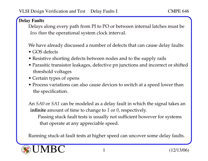
VLSI Design Verification and Test Delay Faults I CMPE 646 Delay Faults Delays along every path from PI to PO or between internal latches must be less than the operational system clock interval. We have already discussed a number of defects that
VLSI Design Verification and Test Delay Faults I CMPE 646 Delay Faults Delays along every path from PI to PO or between internal latches must be less than the operational system clock interval. We have already discussed a number of defects that can cause delay faults: • GOS defects • Resistive shorting defects between nodes and to the supply rails • Parasitic transistor leakages, defective pn junctions and incorrect or shifted threshold voltages • Certain types of opens • Process variations can also cause devices to switch at a speed lower than the specification. An SA0 or SA1 can be modeled as a delay fault in which the signal takes an infinite amount of time to change to 1 or 0 , respectively. Passing stuck fault tests is usually not sufficient however for systems that operate at any appreciable speed. Running stuck-at fault tests at higher speed can uncover some delay faults. L A N R Y D UMBC A B M A L T F O U M B C I M Y O R T 1 (12/13/06) I E S R C E O V U I N N U T Y 1 6 9 6
VLSI Design Verification and Test Delay Faults I CMPE 646 Delay Tests • Delay tests consist of vector-pairs . • All input transitions occur at the same time. • The longest delay combinational path is referred to as the critical path , which determines the shortest clock period. A delay fault means that the delay of one or more paths (not necessarily the critical path) exceeds the clock period. Test Definition: • At time t 1 , the initializing vector of the two-pattern test, V 1 , is applied through the input latches or PIs and the circuit is allowed to stabilize. • At time t 2 , the second test pattern, V 2 , is applied. • At time t 3 , a logic value measurement (a sample) is made at the output latches or POs. The delay test vectors V 1 and V 2 may sensitize one or more paths, p i . L A N R Y D UMBC A B M A L T F O U M B C I M Y O R T 2 (12/13/06) I E S R C E O V U I N N U T Y 1 6 9 6
VLSI Design Verification and Test Delay Faults I CMPE 646 Delay Tests Let: • T C = (t 3 - t 2 ) represent the time interval between the application of vector V 2 at the PIs and the sampling event at the POs • The nominal delay of each of these paths be defined as pd i . • The slack of each path be defined as sd i = T C - pd i . This is the difference between the propagation delay of each of the sensi- tized paths in the nominal circuit and the test interval. Transient region From FFs or PIs Combinational Logic Slack To FFs or POs Delay of combination logic Clock period cannot exceed the clock period t 2 t 3 L A N R Y D UMBC A B M A L T F O U M B C I M Y O R T 3 (12/13/06) I E S R C E O V U I N N U T Y 1 6 9 6
VLSI Design Verification and Test Delay Faults I CMPE 646 Delay Fault Test Generation Difficulties with delay fault test generation: • Test generation requires a sensitized path that extends from a PI to a PO. • Path selection heuristics must be used because the total number of paths is exponentially related to the number of inputs and gates in the circuit. • The application of the test set must be performed at the rated speed of the device. This requires test equipment that is capable of accurately timing two- vector test sequences. • The detection of a defect that introduces an additional delay, ad i , along a sen- sitized path is dependent on satisfying the condition: ad i > sd i (or pd i + ad i > T C ) L A N R Y D UMBC A B M A L T F O U M B C I M Y O R T 4 (12/13/06) I E S R C E O V U I N N U T Y 1 6 9 6
VLSI Design Verification and Test Delay Faults I CMPE 646 Hazards A path sensitized by a delay test consists of on-path nodes and off-path nodes. The nodes along the sensitized path are referred to as on-path nodes. Static sensitization defines the case when all off-path nodes settle to non-con- trolling values (0 for OR/NOR, 1 for AND/NAND) following app. of V 2 . This is a necessary condition to test a path for a delay fault. The gates along the sensitized path have exactly one on-path input and zero or more non-controlling off-path inputs. Delay fault tests are classified according to the voltage behavior of the off-path nodes. Such tests can be invalidated under certain conditions. Hazards can invalidate tests: • Static hazard : describes a circuit condition where off-path nodes change momentarily when they are supposed to remain constant. • Dynamic hazard : describes a circuit condition where off-path nodes make several transitions when they are supposed to make a single transition. L A N R Y D UMBC A B M A L T F O U M B C I M Y O R T 5 (12/13/06) I E S R C E O V U I N N U T Y 1 6 9 6
VLSI Design Verification and Test Delay Faults I CMPE 646 Hazards Static Hazards: ( • ) ( • ) F A B C B = + Glitch on output F G 2 1/1 A D D 1 1/0 B G 4 G 1 E 0/1 F 1 1 G 3 F 1 1/1 C E 0 1 2 3 4 Gate delays are circled. Time line starting when vector ABC = ( 101 ) is applied. Two vector sequence is ABC = ( 111 ), ( 101 ). Gate G 1 introduces an additional delay of 1 unit. Output E of gate G 3 is driven to a logic 1 , one time unit behind D -> 0 . Produces a glitch on F . L A N R Y D UMBC A B M A L T F O U M B C I M Y O R T 6 (12/13/06) I E S R C E O V U I N N U T Y 1 6 9 6
VLSI Design Verification and Test Delay Faults I CMPE 646 Hazards Dynamic Hazards: Glitch on output F ( • ) ( • ) F A B A B = + C G 2 0/1 D 3 1/0/1 G 1 1/0/1/0 A D C F 1/0 1 1 E B G 3 G 4 E 0/1 1 1/1 F Tested path 0 5 1 2 3 4 Time line starting when vector AB = ( 11 ) is applied. Two vector sequence is AB = ( 01 ), ( 11 ). Gate G 2 has a delay value of 3 time units. L A N R Y D UMBC A B M A L T F O U M B C I M Y O R T 7 (12/13/06) I E S R C E O V U I N N U T Y 1 6 9 6
VLSI Design Verification and Test Delay Faults I CMPE 646 Hazards and Invalidation Static hazards can create dynamic hazards along tested paths and need to be considered during test generation. Increasing delay fault size Fault-free Fault detected Test invalidated Fault detected T C V 2 applied (t 1 ) Output Sample Time (t 2 ) Note, unlike the previous example, the glitch occurs before the intended transition, and can invalidate the test (e.g. fault is not detected). L A N R Y D UMBC A B M A L T F O U M B C I M Y O R T 8 (12/13/06) I E S R C E O V U I N N U T Y 1 6 9 6
VLSI Design Verification and Test Delay Faults I CMPE 646 Delay Tests and Invalidation The critical path(s) of this circuit is 6 time units. Let’s set the clock period T = 7. 1 A 3 1 q h 2 4 6 K 1 j B e g P1: A-h-K 2 3 C P2: B-e-q-h-K P3: B-e-g-j-K 2 5 Assume only one faulty path. No delay fault is detected if path delay along P3 is less than 7 units. This test will not detect single delay faults along paths P1 or P2. Assume there can be multiple faulty paths. Assume P2 and P3 are faulty and P2 extends the "static glitch" at the out- put beyond 7 units, then it masks P3’s delay fault. This test is called a non-robust test for delay fault P3. L A N R Y D UMBC A B M A L T F O U M B C I M Y O R T 9 (12/13/06) I E S R C E O V U I N N U T Y 1 6 9 6
VLSI Design Verification and Test Delay Faults I CMPE 646 Delay Fault Path Classification Most paths in a circuit can be classified as: • Hazard-free robust testable • Robust testable • Non-robust testable Hazard-free robust test G 2 C D 1 G 1 D A C F 1/1 1 1 1/1 B G 3 E G 4 1 0/0 F E Off-path inputs do not change. 0 1 2 3 4 Off-path inputs are stable and hazard-free throughout the test interval, T C . This is the most desirable test since invalidation is not possible. L A N R Y D UMBC A B M A L T F O U M B C I M Y O R T 10 (12/13/06) I E S R C E O V U I N N U T Y 1 6 9 6
VLSI Design Verification and Test Delay Faults I CMPE 646 Robust Test Hazard-free robust tests are desirable but it’s not possible in many cases to generate them. Transitions that occur at fan-out points often reconverge as off-path inputs along the tested path. However, robust tests are still possible even when static hazards are present on the off-path inputs. Static hazards are necessary but not sufficient to make a delay test non- robust. A delay test is a robust test if the on-path nodes control the first occurrence of a transition through all gates along the tested path. This ensures that a delay test is not invalidated or a path delay fault masked by delay characteristics of gates not on the tested path. A robust path-delay test guarantees to produce an incorrect value at the out- put if the delay of the path exceeds the clock period, irrespective of other path delays. L A N R Y D UMBC A B M A L T F O U M B C I M Y O R T 11 (12/13/06) I E S R C E O V U I N N U T Y 1 6 9 6
Recommend
More recommend
Explore More Topics
Stay informed with curated content and fresh updates.


