UMBC A B M A L T F O U M B C I M Y O R T 1 - PowerPoint PPT Presentation
Programmable Logic Devices Verilog VIII CMPE 415 Synthesis of Sequential Logic A Verilog description of sequential logic can be synthesized only if certain conditions are met. In general, the event control expression of a cyclic behavior must
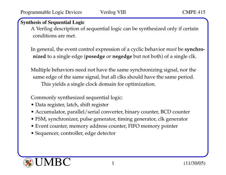
Programmable Logic Devices Verilog VIII CMPE 415 Synthesis of Sequential Logic A Verilog description of sequential logic can be synthesized only if certain conditions are met. In general, the event control expression of a cyclic behavior must be synchro- nized to a single edge ( posedge or negedge but not both) of a single clk. Multiple behaviors need not have the same synchronizing signal, nor the same edge of the same signal, but all clks should have the same period. This yields a single clock domain for optimization. Commonly synthesized sequential logic: • Data register, latch, shift register • Accumulator, parallel/serial converter, binary counter, BCD counter • FSM, synchronizer, pulse generator, timing generator, clk generator • Event counter, memory address counter, FIFO memory pointer • Sequencer, controller, edge detector L A N R Y D UMBC A B M A L T F O U M B C I M Y O R T 1 (11/30/05) I E S R C E O V U I N N U T Y 1 6 9 6
Programmable Logic Devices Verilog VIII CMPE 415 Synthesis of Latches Level-sensitive behavior is characterized by an output that is affected by the input only while a control signal is asserted . Otherwise, the input is ignored and the output remains constant. Synthesis tools infer a latch when they • Detect a level-sensitive behavior (no edge constructs) • A register variable is assigned value in some threads of activity but not oth- ers, e.g., an incomplete if stmt. The synthesis tool must identify the datapaths and their control signals. The control signal is the signal whose value controls the branching of the activity flow to the stmts that assign/don’t assign value to a reg variable. If a register is assigned value in all activity flows, a latch is inferred if a path assigns a variable its own value, i.e., if it has feedback . Otherwise, it’s combinational. L A N R Y D UMBC A B M A L T F O U M B C I M Y O R T 2 (11/30/05) I E S R C E O V U I N N U T Y 1 6 9 6
Programmable Logic Devices Verilog VIII CMPE 415 Synthesis of Latches General rules: • Latches implement incompletely-specified assignments in case and if stmts. • If a case stmt has a default assignment in which the variable is explicitly assigned to itself, synthesis will choose a MUX structure with feedback. • If an if stmt assigns a variable to itself, a MUX with feedback is used. • If the behavior is edge-sensitive , incomplete case and if stmts synthesize to FFs. • If feedback is present, the FF output is fed back using MUX. • A latch is inferred when the conditional operator, ? ... :, is implemented with feedback. Actual implementation depends on the context. If conditional operator is used in a continuous assignment , the result is a MUX with feedback. If used in an edge-sensitive cyclic behavior, the result is a register with a gated datapath in a feedback configuration. If used in a level-sensitive cyclic behavior, the result is a hardware latch. L A N R Y D UMBC A B M A L T F O U M B C I M Y O R T 3 (11/30/05) I E S R C E O V U I N N U T Y 1 6 9 6
Programmable Logic Devices Verilog VIII CMPE 415 Synthesis of Latches Be aware that explicit gate-level latches, e.g., cross-coupled nand gates, and other combinational feedback, will not be synthesized into hardware latches. The synthesis tools will detect this and issue a warning. Here, the case list is incomplete (only 5 of 8) module latch_case_assign(latch_out, latch_in, set, clear, enable); input latch_in, enable, set, clear; output latch_out; reg latch_out; always @(enable or set or clear) case ({enable, set, clear}) 3’b000: assign latch_out = latch_in; //Transparent mode 3’b110: assign latch_out = 1’b1; // Set 3’b010: assign latch_out = 1’b1; // Set 3’b101: assign latch_out = 1’b0; // Clear 3’b001: assign latch_out = 1’b0; // Clear default : deassign latch_out; // Hold residual value endcase endmodule Simulates efficiently but does not synthesize by all tools. L A N R Y D UMBC A B M A L T F O U M B C I M Y O R T 4 (11/30/05) I E S R C E O V U I N N U T Y 1 6 9 6
Programmable Logic Devices Verilog VIII CMPE 415 Synthesis of Latches This one is synthesizable by all tools but yields feedback logic. module latch_case1(latch_out, latch_in, set, clear, enable); input latch_in, enable, set, clear; output latch_out; reg latch_out; always @(enable or set or clear or latch_in) // latch_in in activity list. case ({enable, set, clear}) 3’b000: assign latch_out = latch_in; 3’b110: assign latch_out = 1’b1; 3’b010: assign latch_out = 1’b1; 3’b101: assign latch_out = 1’b0; 3’b001: assign latch_out = 1’b0; default : latch_out = latch_out; // Explicit assignment of residual value endcase endmodule set clear latch_out latch_in MUX enable L A N R Y D UMBC A B M A L T F O U M B C I M Y O R T 5 (11/30/05) I E S R C E O V U I N N U T Y 1 6 9 6
Programmable Logic Devices Verilog VIII CMPE 415 Synthesis of Latches This one is synthesizable by all tools and generates a latch. module latch_case2(latch_out, latch_in, set, clear, enable); input latch_in, enable, set, clear; output latch_out; reg latch_out; always @(enable or set or clear or latch_in) // latch_in in activity list. case ({enable, set, clear}) 3’b000: assign latch_out = latch_in; 3’b110: assign latch_out = 1’b1; 3’b010: assign latch_out = 1’b1; 3’b101: assign latch_out = 1’b0; // Incomplete specification 3’b001: assign latch_out = 1’b0; endcase endmodule latch_out latch_in clear enable Latch set MUX L A N R Y D UMBC A B M A L T F O U M B C I M Y O R T 6 (11/30/05) I E S R C E O V U I N N U T Y 1 6 9 6
Programmable Logic Devices Verilog VIII CMPE 415 Synthesis of Latches As another example: module latch_if1(data_out, data_in, latch_enable); input [3:0] data_in; output [3:0] data_out; input latch_enable; // MUX with feedback reg [3:0] data_out; always @(latch_enable or data_in) if (latch_enable) data_out = data_in; else data_out = data_out; endmodule assign data_out[3:0] = latch_enable ? data_in[3:0] : data_out[3:0]; module latch_if2(data_out, data_in, latch_enable); input [3:0] data_in; output [3:0] data_out; input latch_enable; // Incompletely specified reg [3:0] data_out; // yields an array of latches. always @(latch_enable or data_in) if (latch_enable) data_out = data_in; endmodule L A N R Y D UMBC A B M A L T F O U M B C I M Y O R T 7 (11/30/05) I E S R C E O V U I N N U T Y 1 6 9 6
Programmable Logic Devices Verilog VIII CMPE 415 Synthesis of FFs A register variable will be synthesized into a FF (a memory element) if • It is referenced outside the scope of the behavior. • It is referenced within a behavior before it is assigned value • It is assigned value in only some branches of the activity. A register will be synthesized as the output of a FF when its value is assigned synchronously with the edge of a signal. By decoding signals immediately after the event control expression allows the synthesis tool to determine: • Which of the edge-sensitive signals are control signals • Which is the synchronizing signal. If the event control expression is sensitive to the edge of more than one signal, an if stmt must be the first stmt in the behavior. The control signals must be decoded explicitly in the branches of the if stmt. Decode the reset condition first. L A N R Y D UMBC A B M A L T F O U M B C I M Y O R T 8 (11/30/05) I E S R C E O V U I N N U T Y 1 6 9 6
Programmable Logic Devices Verilog VIII CMPE 415 Synthesis of FFs The synchronizing signal is not tested explicitly in the body of the if stmt, but by default, the last branch must describe the synchronous activity. module swap_synch(set1, set2, clk, data_a, data_b); output data_a, data_b; input clk, set1, set2; reg data_a, data_b; always @( posedge clk) begin if (set1) begin data_a <= 1; data_b <= 0; end else if (set2) begin data_a <= 0; data_b <= 1; end else begin data_b <= data_a; //These assignments implicitly data_a <= data_b; // synchronized with rising edge end // of clk end endmodule See text for synthesized circuit, which includes two FFs and logic to explicitly decode set1 and set2 . The outputs of the FFs are feedback to implement else . L A N R Y D UMBC A B M A L T F O U M B C I M Y O R T 9 (11/30/05) I E S R C E O V U I N N U T Y 1 6 9 6
Programmable Logic Devices Verilog VIII CMPE 415 Synthesis of FFs As we have seen, not every register variable synthesizes to a hardware stor- age device, e.g., the nand gate example covered previously. Here temp is used only within the behavior and is not referenced before it is assigned value. In this example, the synthesis tool is able to correctly infer the need for a resettable FF. module D_reg4_a(Data_in, clock, reset, Data_out); input [3:0] Data_in; input clock, reset; output [3:0] Data_out; reg [3:0] Data_out; always @( posedge clock or posedge reset) begin if (reset == 1’b1) Data_out <= 4’b0; else Data_out <= Data_in; end endmodule L A N R Y D UMBC A B M A L T F O U M B C I M Y O R T 10 (11/30/05) I E S R C E O V U I N N U T Y 1 6 9 6
Recommend
More recommend
Explore More Topics
Stay informed with curated content and fresh updates.


