The pn junction [Fonstad, Ghione] Band diagram On the vertical - PowerPoint PPT Presentation
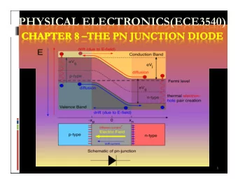
The pn junction [Fonstad, Ghione] Band diagram On the vertical axis: potential energy of the electrons On the horizontal axis: now there is nothing: later well put the position q F s : work function ( F s : extraction potential),
The pn junction [Fonstad, Ghione]
Band diagram On the vertical axis: potential energy of the electrons On the horizontal axis: now there is nothing: later we’ll put the position q F s : work function ( F s : extraction potential), depends on doping (which moves E F ) q c s : electron affinity (~ 4 eV for Si) E 0 : vacuum level Now we’ll consider the band diagrams in thermal equilibrium only
The same material, with different doping If the two samples are isolated from each other, we have -> note: the electron affinity does not change We’ll first assume uniform doping in each sample The work function is larger for the p side p side n side
The same material, with different doping We have a junction ! How to build the band diagram: the Fermi level is constant (if not, electrons would move from zones with higher f(E) to zones with lower f(E), due to the different probability of occupation of the states) electron affinity and forbidden gap width are constant (depend on the material only) far from the junction, the band structure is that of the isolated material the vacuum level is continuous
Band diagram in contact 1 st approx. drawing... complete drawing E 0 is now the energy of the electron just outside the material
Depletion region Where bands bend, there are two depletion layers, where r ~ N D or r ~ N A These are space-charge regions => E => potential The contact potential, or built-in potential, is in order to compute the width of the depletion region, we’ll compute with ( global neutrality)
The two components of the built-in potential V i
Depletion region and potentials Two integration steps: - [ div E = r/e 0 ] constant r => linear E (x) - [ E =-dv/dx ] linear E (x) -> parabolic j (x) j: electric potential – conventionally referred to E Fi U : potential energy of the electrons at E Fi (well, they do not exist...) U=-q j U is also (apart from an offset) the potential energy of the electrons e.g. at the bottom of CB
Depletion region So we get so that And we get with N A x p =N D x n and N eq =(N A N D )/(N A +N D ) So, higher doping => thinner depletion region
Out of thermal equilibrium Reverse bias....................................... forward bias
Out of thermal equilibrium
<-- minus! Electrons potential energy and concentrations E and j in the depletion region -> E => we have to spend energy to move electrons from right to left i.e. their potential energy U increases when moving from right to left U has the same behaviour of E Fi (and the same of j but with opposite sign) So from [sl. 110/24] we can write
The current Let us consider a 1D model (i.e., the section is constant along x ) Hypothesis: low injection n, p neglectable in the depletion layers the sides of the junctions ( w p , w n ) are much longer than the diffusion lengths L n =(D n t n ) 1/2 and L p =(D p t p ) 1/2 In any section dr dr low injection -> We need to compute the concentrations of minority carriers
Junction law The solutions of the diffusion equations are here We need to know n’ p (-x p ) and p’ n (x n ) From we get
Junction law From we get At equilibrium ( V =0) Out of equilibrium (but with low injection): junction law ->
Out of equilibrium Carriers profile ->
The current E.g. at x=x n J tot (x n )=J p (x n )+J n (x n )=J p, diff (x n )+J n (x n ) Assuming that recombination is neglectable in the space charge region , J n (x n )=J n (-x p )=J n, diff (-x p ) so that J tot (x n )=J p, diff (x n )+J n, diff (-x p ) p n n p
The current And we finally get with
Effect of temperature Higher T implies higher current, due to changes in - increase in carrier concentration - V T - changes in D n/p and L n/p At constant voltage, I doubles for an increase of 10 o C At constant current, V decreases of about 2.5 mV/ o C
Depletion (or transition) capacitance Due to variations in the width of the depletion layer -> variations of the charge
Diffusion capacitance Due to variations in the profile of the carriers in the proximity of the depletion layer The “extra” charge in the profile of the carriers concentrations, close to the space charge region, is proportional to J : The corresponding capacitive effect is also proportional to J :
Diodes and switching [See spice Simulation]
Large signal model So the large signal model of a diode is -> All these 3 parameters (1 conductance and 2 capacitors) change with bias In inverse bias C j prevails on C d the opposite in direct bias
Small signal model By linearising the model around the bias point we obtain the small signal model -> g d0 =I/ h V T where I is the bias current It is a linear model!
Zener diodes All diodes are subject to breakdown for sufficiently high inverse bias Zener diodes are designed to work in this condition, normally as voltage references Two physical mechanisms: tunnel and avalanche Higher doping => thinner depletion region => higher E => easier breakdown => lower V z In order to have higher V z : lower doping (at least on one side)
Tunnel and avalanche breakdown Tunnel: for V Z <6V, high doping; V Z decreases with T Avalanche: for V Z >6V, lower doping; V Z increases with T
Photodiodes • If suitable photons reach the junction, they I may generate electron-hole couples V • minority (and also majority) concentrations will increase • In reverse bias, current will be larger due to an extra photo-generated current I S proportional to the # of photons • and we have I = -I S + I 0 (exp V/V T -1) • Photodiodes can be used as light detectors I’ • Considering the opposite current ( I’= -I ) V
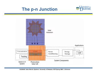
Photodiodes as power generators I’ V • So we have an open circuit voltage I’ (photovoltaic effect) V • and a short circuit current I’ V • And we can also extract power! • Photovoltaic cells are diodes with very large area (to get many I’ V photons), optimized for power generation
LEDs
LEDs [Please note: the right drawing is deceitful, electron and holes are on the lines, not above or below the lines]
Heterojunctions E G ~1.4 eV for GaAs E G ~1.7 eV for AlGaAs Isolated semiconductors 1. Ideally, immediately after junction 2. (1) creation At thermal equilibrium 3. (2) (3)
Recommend
More recommend
Explore More Topics
Stay informed with curated content and fresh updates.


