The ATLAS Upgrade Introduction Planar Pixel Sensor R&D Project - PowerPoint PPT Presentation
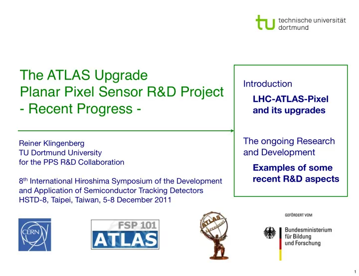
The ATLAS Upgrade Introduction Planar Pixel Sensor R&D Project LHC-ATLAS-Pixel - Recent Progress - and its upgrades The ongoing Research Reiner Klingenberg and Development TU Dortmund University for the PPS R&D Collaboration
The ATLAS Upgrade Introduction Planar Pixel Sensor R&D Project LHC-ATLAS-Pixel - Recent Progress - and its upgrades The ongoing Research Reiner Klingenberg and Development TU Dortmund University for the PPS R&D Collaboration Examples of some recent R&D aspects 8 th International Hiroshima Symposium of the Development and Application of Semiconductor Tracking Detectors HSTD-8, Taipei, Taiwan, 5-8 December 2011 1
Large Hadron Collider and the ATLAS Experiment so far: LHC collides p+p at 3.5 + 3.5 TeV some 1300 bunches with 2·10 14 protons instantaneous luminosity ~ 3·10 33 cm -2 s -1 or ~ 3 kHz/µb 2
ATLAS - Pixel Detector innermost detector component 3 barrel layers + 2·3 endcap disks covers pseudorapidity range | η | < 2.5 Performance requirements transverse impact resolution < 15 µm minimal material to reduce multiple scattering and conversions high efficiency radiation hard: 500 kGy, 10 15 n eq cm -2 Module concept detector consists of 1744 modules of planar silicon n + -in-n sensors + frontend electronics FE-I3+ flex hybrid ~80 millions read-out channels 3
ATLAS - Pixel Detector Pixel Sensor Design DOFZ Si n-substrate, 250 µm thick planar n + -in-n pixels, 400x50 µm 2 16 guard rings on p side to reduce HV in steps 1.1 mm inactive edge incl. safety margin Read-out electronics FE-I3 chip DC coupled and bump bonded shaper + amplifier + discriminator ⇒ ToT ⇒ charge Q 4
Challenges at High Luminosity LHC : goal to extend physics reach with increased peak luminosity to increase sensitivity for physics beyond the standard model like Higgs, SUSY, extra dimensions, heavy bosons Detectors increased occupancy and high event rate O(100) events / bunch crossing event pile-up ⇒ challenging reconstruction higher pixel granularity Radiation damage ⇒ charge collection, depletion fluences of 10 16 n eq cm -2 in inner layer radiation hard material, design of sensor layout, thinness of bulk, higher bias voltage, lower threshold in read-out electronics 5
Envisaged LHC and ATLAS Upgrade Phases phase 0: IBL Insertable b-Layer phase I: NewPix under evaluation now phase II: New Inner Detector first step: IBL, increasing luminosity the Insertable B-Layer ➥ radiation hardness increasing occupancy ➥ better granularity required 6
ATLAS Planar Pixel Sensor Project Goals Tools different sensors : CiS / HLL-MPI / evaluate & improve efficiencies & charge MICRON / HPK and read-out FEI3/FEI4 performances @ high & highest fluences V bia 0 ⇒ radiation hardness? operation conditions 50x250 n + -pixels 50x250 3-21 n + -pixels n-substrat, DOFz, 75-250 75-250 p-substrat, Fz, 3-16 0 V bias > V bias > geometry optimization ⇒ pixel size; pixel implant; bias grid n&p irradiations (Ljubljana reactor n, CERN 24 GeV p, Karlsruhe 26 MeV p, slim/active edges; LANL 800 MeV p) up to 2·10 16 n eq cm -2 dicing characterisation in lab and test beams CERN 120 GeV π DESY 4 GeV e cost reduction at large areas ⇒ bulk options & bump bonding FE Cu 3 Sn Cu 6 Sn 27 µ m TCAD simulations and dopant profile Sens measurements for optimization 7
Sensors measured in lab and test beam sensors bonded to FE-I3 or FE-I4 read-out chips are tested in the laboratory with the help of radioactive sources and in a test beam set-up equipped with a beam telescope which allows tracking test beam: hit maps & energy deposition & efficiencies single chip & spatial resolution adapter card w/ sensor+FE EUDET Reports 2010-01 & 2008-04 one or several DUTs cooling source scans: hit maps & energy deposition 8
n + -in-n sensors: collected charge after neutron irradiations are currently used in the ATLAS pixel detector for a fluence range 10 15 n eq cm -2 tests of the radiation hardness of up to 2 ⋅ 10 16 n eq cm -2 are ongoing neutron irradiation (Ljubljana reactor) up to 2 ⋅ 10 16 n eq cm -2 , FE-I3 read-out measurements with e - from 90 Sr source and π &e test beam 5·10 15 n eq cm -2 (n) 2·10 16 n eq cm -2 (p) charges seen are higher than model predictions which include trapping 9
n + -in-n sensors: collected charge after proton irradiations proton irradiation (KIT, 26MeV) up to 1.4 ⋅ 10 16 n eq cm -2 , FE-I3 read-out unirradiated FE with indium bumps flip-chipped to irradiated sensor measurements with e - from 90 Sr source and π test beam 1·10 16 n eq cm -2 (p) 1.4·10 16 n eq cm -2 (p) cluster charge threshold FE-I3 3200e - 10
n + -in-n sensors: hit efficiencies after neutron & proton irradiations CiS 250 µm + 285 µm hit efficiency can be fully recovered by increasing bias voltage (5-20)·10 15 n eq cm -2 (n) (2-14)·10 15 n eq cm -2 (p) O(10 15 ) n eq cm -2 % O(10 16 ) n eq cm -2 charge distributions @ 1.4·10 16 n eq cm -2 (p) 11
n + -in-n sensors: hit efficiencies after neutron & proton irradiations sub-pixel resolved hit efficiency sub-pixel resolved hit efficiency for a for a 250 µm sensor 250 µm sensor @ 1.4 ⋅ 10 16 n eq cm -2 (p) @ 4 ⋅ 10 15 n eq cm -2 (n) mean efficiency > 97% @ 1800 V mean efficiency > 97% @ 600 V 1800V 1300V LUB2 12
n-in-p sensors NIM ¡A ¡636 ¡(2011) ¡56 strips V bias 0 V 50x250 µ 3-21 GR n + -pixels p-substrat, Fz, MCz 75-250 µm p + -implant V bias > 500V investigation of charge multiplication parallel ¡ row wire ¡bondable ¡ pixels pixels parallel ¡ column 6’’ ¡300µm ¡wafers, ¡double ¡metall, ¡n-‑in-‑p ¡FZ 300 µm - 140 µm has been investigated effect more significant in thin sensors 13
n-in-p sensors lab data assemblies were irradiated up to 5 ⋅ 10 15 n eq cm -2 , neutrons and mixed significant charge is collected above threshold, V bias > 600V FE-I3 threshold 5·10 15 n eq cm -2 V bias =1kV 14
n-in-p sensors lab + test beam 300 µm, BCB insulation on pixel side, HV stability proven n-irradiation @ 5 ⋅ 10 15 n eq cm -2 : significant charge is collected above threshold lab and test beam measurements deliver comparable results Vbias = 600V 98.6% MPV(charge)=6.4ke overall efficiency 98.6% losses around bias dot 99.8% higher eff in the center of the pixels 15
150 µm Thin bulk sensors first HPK n-in-p sensors, 150 µm, 6’’ wafer FE-‑I3 ¡1-‑chip ¡pixels with different pixel biasing and isolations bias structure aims to reduce less-efficient area Punch-thru PTLA (a bias-dot in the 4-corner) FE-‑I4 ¡2-‑chip ¡pixels PolySilicon (no bias dot, encircling pixel implant, ~2 M Ω ) FE-‑I4 ¡1-‑chip ¡pixels isolation structure FE-‑I3 ¡4-‑chip ¡pixels p-stop ~4·10 12 ions cm -2 , Common & Individual p-spray ~2·10 12 ions cm -2 HPK ¡n-‑in-‑p ¡6-‑in. ¡wafer PTLA IsolaCon ¡scheme have been Bias ¡rail Biasing investigated Scheme in test beams PolySi 16
150 µm Thin bulk sensors: test beam results #3 #4 non-irrad: FDV~40 V, saturated > 40 V 1 [μm] operated at 150 V bias voltage in test beam shown are sub-pixel resolved efficiency of non-irradiated FE-I4 samples [μm] p-stop common on Poly Silicon shows best p-‑stop ¡individual, ¡Poly-‑Si p-‑stop ¡common, ¡Poly-‑Si efficiency map #5 #6 slight inefficiency beneath the bias rail 8 6 4 2 0 8 “ToT charge” in arbitrry units 6 4 2 0 p-‑stop ¡individual, ¡PTLA p-‑stop ¡common, ¡Poly-‑Si Q ¡[e] ¡(Arbitrary ¡unit) 2D ¡efficiency ¡map ¡of ¡a ¡pixel, ¡non-‑irrad, ¡at ¡150 ¡V ¡bias ¡voltage 4 FE-I4 samples also investigated after irradiation 2·10 15 n eq cm -2 (FE-I4) black ¡ ¡ ¡: ¡avg. ¡non-‑irradiated red ¡ ¡ ¡ ¡: ¡avg. ¡irradiated 2x PolySi-common p-stop: KEK4,5 PolySi-individual p-stop: KEK3 PTLA-individual p-stop: KEK6 Bias ¡voltage ¡[V] Bias ¡voltage ¡dependence ¡of ¡collected ¡charges Note: ¡independent ¡charge ¡calibraCon ¡for ¡non-‑irradiated ¡and ¡irradiated ¡samples. ¡ ¡ 17
Slim edges: DRIE control potential drop along edge cut and reduce inactive area DRIE (Deap Reactive Ion Etching, CNM/IFAE, FBK/LPNHE, VTT/MPI&LAL) needs deep trenches, aspect ratio (1:20) polysilicon filling width of 8-12µm encouraging results on FBK test diodes electrical characteristics rely on well defined trenches; ongoing improvements doi:10.1016/j.nima.2011.04.050 18
Slim edges: SCP Laser scribe & cleave & edge passivation keeps edge as a clean crystal boundary passivation defines edge state and prevents conductive channels by SiO 2 oxide growth for n-type 100-wafers in production atomic layer deposition or Al 2 O 3 for p-type encouraging results; in collaboration with US Navel Research Lab also see presentation by Marc Christophersen 19
Slim edges minimize inactive area , avoids shingling along beam axis shifting pixel beneath guard rings CiS n + -in-in with slim edges, 250 µm irradiated to 4·10 15 n eq cm -2 data from pion test beam @ CERN significant part of edge pixel sensitive depends on HV and thickness inactive edge reduced down to ~ 200 µm design chosen for the planar IBL sensor Edge efficiency LUB2 4·10 15 n eq cm -2 (n) 20
Recommend
More recommend
Explore More Topics
Stay informed with curated content and fresh updates.
