STM and spectroscopy of nanosized ferromagnetic structures - PowerPoint PPT Presentation
School on magnetism, Cluj, September 2007 STM and spectroscopy of nanosized ferromagnetic structures Guillemin Rodary (Max Planck Institute, Halle, Germany) Ferromagnetic nanostructures L sample L exch L domain wall Gas phase
School on magnetism, Cluj, September 2007 STM and spectroscopy of nanosized ferromagnetic structures Guillemin Rodary (Max Planck Institute, Halle, Germany)
Ferromagnetic nanostructures • L sample ≈ L exch ≈ L domain wall Gas phase nucleation ⇒ monodomaine (Stoner-Wohlfarth switching ?) Bonet,PRL 83, 4188 (1999) • Temperature could overcome anisotropy kT ≈ KV ⇒ superparmagnetism Bean, JAP 30, 120S (1959) Néel, Ann. Geopgys. 5, 99 (1949) Jamet, PRB 69, 024401 (2004). • Atoms with low coordination Thermal evaporation ⇒ K surface or M could be very high Gambardela, Science 300, 1130 (2003) • Quantum effects (discrete states, collective tunneling) Bernand-Mantel , APL 89, 062502 (2006) Wernsdorfer,PRL 79, 4014 (1997) 50 nm
Probing nanomagnetism Imaging See review Freeman, Science 294, 1484 (2001) Sensitive to Typical resolution Specificity MOKE M 500nm Easy to use and cheap Argyle, JAP 87, 6487 (2000) XMCD-PEEM M <10nm Element specific, dynamic, synchrotron Vogel, PRB 72, 220402 (2005) SEMPA M 10nm Vectorial M, surface Allenspach, JMMM 129, 160 (1994) ∇ B Lorentz <10nm Average over sample, no field Chapman, JMMM 200, 729 (1999) ∇ B MFM 50nm Insulator OK, not quantitative Folks, APL 76, 909 (2000) SP-STM TMR <1nm No insulator, smooth surface, topography and spectro Magnetometry • SQUID, MOKE: thin films: OK nanoparticles : average over an assembly of identical objects Rohart, PRB 73, 165412 (2006) • µ-SQUD: able to measure the switching field of a single nanostructure Jamet, PRB 69, 024401 (2004) Spin dependant transport Bernand-Mantel , APL 89, 062502 (2006) Lithography allows to take contact up to 10~100nm Ralph, PRL 74, 3241 (1995)
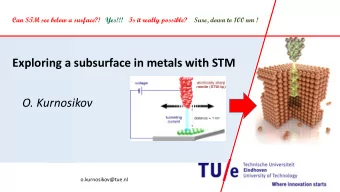
Scanning tunneling microscopy V Surface Tip Barrier φ eV d − φ − ∝ d eV I e tunnel Topography image a constant current
Scanning tunneling microscopy V Surface Tip Barrier φ eV d − φ − ∝ d eV I e tunnel Topography image a constant current
Scanning tunneling microscopy V Surface Tip Barrier φ eV d − φ − ∝ d eV I e tunnel Topography image a constant current
Scanning tunneling microscopy Ultra high vacuum: 10 -11 mbar Low temperature: T = 4 K V High magnetic field: B= 8 T → Surface science, Surface electronic properties and nanomagnetism Tip Barrier φ eV d − φ − ∝ d eV I e tunnel Topography image a constant current
Growth of nanostructures studied by STM Nanodots Nanopillars 1D chains Co/Au(788) Co/Au(111) Co/Pt(997) Repain, EPL 58, 730 (2002) Fruchart, PRL 83, 2769 (1999) Gambardella, JPhysCondMat 15, 2533 (2003) 480K 280K 130K 150 nm • Chains width of 1, 2 or 3 atoms 60 nm • Temperature growth ⇒ • Ferromagnetic behavior with • 3D structures very high magnetic moment Diffusion coefficient + trap energy • Aspect ration 2:1 • Reduce dimensionality ⇒ • Periodical array of similar dots ⇒ • Blocking temperature: strong magnetic anisotropy from 20 K to 300K Array = N x single dot
Scanning tunneling spectroscopy ( ) LDOS map ∫ eV ∝ ε I ( r ) LDOS r , E d → Electronic structures tunnel 0 = ∑ ( ) ψ 2 δ E − LDOS r , E ( r ) ( E ) ν ν ν d I ( ) ∝ ( r , E ) LDOS r , E d V Density of electronic states Co on Cu, 40x40nm available for tunneling Point spectroscopy → LDOS at a nanoscale 9 Minority Co state dI/dV (arb. units) 6 Co island Bare Cu (x4) 3 Cu surface state 0 -0.8 -0.4 0.0 0.4 0.8 Voltage (V)
Principle of Spin-Polarized STM Magnetic tunnel junction with vacuum Antiparallel 94 Cr Tip 92 Resistance (k Ω ) 90 Vaccum Parallel 88 Co island 86 High 84 current -0.10 -0.05 0.00 0.05 0.10 Applied field (T) Low current V 1 Bode, Getzlaff, Wiesendanger, Phys. Rev. Lett. 81, 4256 (1998). Wulfhekel, Kirschner, Appl. Phys. Lett. 75, 1944 (1999)
Principle of Spin-Polarized STM Magnetic tunnel junction with vacuum Antiparallel 94 Cr Tip 92 Resistance (k Ω ) 90 Vaccum Parallel 88 Co island 86 High 84 current -0.10 -0.05 0.00 0.05 0.10 Applied field (T) V 1 Low current V 1 Bode, Getzlaff, Wiesendanger, Phys. Rev. Lett. 81, 4256 (1998). Wulfhekel, Kirschner, Appl. Phys. Lett. 75, 1944 (1999)
Principle of Spin-Polarized STM Magnetic tunnel junction with vacuum Antiparallel 94 Cr Tip 92 Resistance (k Ω ) 90 Vaccum Parallel 88 Co island 86 High 84 current -0.10 -0.05 0.00 0.05 0.10 Applied field (T) V 1 Low current V 1 Bode, Getzlaff, Wiesendanger, Phys. Rev. Lett. 81, 4256 (1998). Wulfhekel, Kirschner, Appl. Phys. Lett. 75, 1944 (1999)
Nanomagnetism: imaging of spin structure Magnetic surface reconstruction - “Spin maps” made at constant current and at fixed voltage - Spin sensitivity of the tip in or out of plane 1ML of Mn on Fe(001) Gao, PRL 98, 107203 (2007)) Single magnetic atoms Magnetic nanostructures In-plane Cr tip Out-of-plane Cr tip Atoms on Co islands Vortex in Fe island on W(110), Wachoviak, Science 298, 577 (2002) Yayon, PRL 99 , 067202 (2007)
Co island on Cu(111) Co deposition at 300K on Cu(111) ⇒ Triangular Co islands ⇒ Step edge decoration 50 x 50 nm 2 , -0.36 V, 1 nA 0.4 Linescan Height (nm) 0.3 2 monolayer high 0.2 island 0.1 750 x 750 nm 2 , -0.8 V, 1 nA 0.0 0 5 10 15 20 25 Position (nm)
Spectroscopy on a single island dI/dV image Point spectroscopy on the island 0.5 dI/dV (arb. units) 0.5 0.0 dI/dV (arb. units) 0.0 -0.5 -0.6 -0.3 0.0 0.3 0.6 -0.5 Asymmetry Faulted island -1.0 Unfaulted island -1.5 50 x 50 nm 2 , -0.36 V, 1 nA -0.6 -0.4 -0.2 0.0 0.2 0.4 0.6 fcc site Hcp site Voltage (V) 1st Cu 2d Cu Faulted Unfaulted 3d Cu Co Vazquez de Parga, Garcia-Vidall, Miranda, PRL 85, 4365 (2000) and Pietzsch, Kubtzka, Bode, Wiesendanger, PRL 92, 057202 (2004)
Spectroscopy on a single island I(V) and dI/dV(V) curves measured at island center Extraction of the hysteresis cycle In field spectroscopy at different voltages 12 10 0 T 10 - 1 T dI/dV (arb. units) 8 dI/dV (arb. units) - 4 T - 1 T 8 6 0 T 6 4 -0.3V 2 4 -0.6V 0 2 -0.75 -0.50 -0.25 0.00 0.25 0.50 0.75 -4 -3 -2 -1 0 1 2 3 4 Voltage (V) Field (T) - TMR hysteresis loop of a single nanostructure - Understanding the relative magnetic orientation of tip and sample - Measure the TMR at a nanoscale
Size dependence of the switching field 7 1.0 T 1.2 T 1.8 T 6 2430 atoms 4210 atoms dI/dV (arb. units) 5 4820 atoms 4 3 2 1 0 1 2 3 4 Regime between superparamgnetism Field (T) and multi-domain island 2.0 Switching field Switching field (T) 1.5 2K/M S 1.0 Monodomaine Multidomaine ~1/V 0.5 Superpara 0.0 Volume 0 2000 4000 6000 Atom number
Conclusion • STM: study of growth, structure and organization of ferromagnetic nanostructures (films, dots, pillars, chains…) 9 Minority Co state • STS: - mapping of the electronic structure (standing waves) dI/dV (arb. units) 6 Co island - locales density of states on nanostructures Bare Cu (x4) - structure caracterisation 3 Cu surface state 0 • SP-STM: - spin map in and out of plane with atomic resolution -0.8 -0.4 0.0 0.4 0.8 Voltage (V) - spin dependant transport (TMR) at a nanoscale - study of switching of a single nanoobject 12 10 dI/dV (arb. units) 8 6 -0.3V 4 -0.6V 2 -4 -3 -2 -1 0 1 2 3 4 Field (T)
Size dependence of the island switching field 2.0 7 6 2430 atoms Switching field (T) 1.5 4210 atoms dI/dU (arb. units) 5 4820 atoms 4 1.0 3 0.5 2 1 0.0 0 2000 4000 6000 0 1 2 3 4 Field (T) Atom number
Observation of Magnetic Hysteresis at the Nanometer Scale by Spin- polarized Scanning Tunneling Spectroscopy O. Pietzsch, A. Kubetzka, M. Bode, R. Wiesendanger, Science 292, 2053 (2001)
L. Niebergall, V. S. Stepanyuk, J. Berakdar, and P. Bruno, PRL 96 , 127204 (2006)
Introduction: context of SP-STM Surface Science Spintronic Scanning tunneling microscope Tunnel Magnetoresitance Atomic resolution Cu(111), 2x2nm Co nanostructure on Cu(111) 50x50nm Co/Al 2 O 3 /NiFe tunnel junction 94 92 Resistance (k Ω ) 90 88 86 84 -0.10 -0.05 0.00 0.05 0.10 Applied field (T) Spin-polarized STM 12 10 dI/dV (arb. units) 8 6 -0.3V 4 -0.6V 2 -4 -3 -2 -1 0 1 2 3 4 Field (T)
9 Minority Co state dI/dV (arb. units) 6 Co island Bare Cu (x4) 3 Cu surface state 0 -0.8 -0.4 0.0 0.4 0.8 Voltage (V)
Principe of TMR Jullière model: Open questions: - Spin is conserved during tunneling - Conductance ∝ DOS of electrodes - TMR sign, depend only of P 1 P 2 ? ↑ ↑ ↓ ↓ ∝ + P - Interface electrode/barrier ? G N . N N . N 1 2 1 2 ↑ ↓ ↓ ↓ ∝ + AP - Voltage dependence ? G N . N N . N 1 2 1 2 - Influence of the DOS ? d ↑ s ↑ d s ↓ ↑ ↓ − N N = d ↓ i i P i ↑ + ↓ N N i i E F − P AP G G ≡ = TMR P 1 P + 2 P AP G G = + G G ( 1 P P cos( M , M ) ) 1 Teresa et al. Science 286, 507 (1999) 0 1 2 2
Recommend
More recommend
Explore More Topics
Stay informed with curated content and fresh updates.
