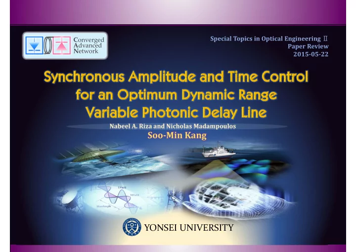
Soo Min Kang YONSEI UNIVERSITY Contents Introduction - PowerPoint PPT Presentation
Special Topics in Optical Engineering C onverged Paper Review A dvanced N etwork 2015 05 22 Nabeel A. Riza and Nicholas Madampoulos Soo Min Kang YONSEI UNIVERSITY Contents Introduction Introduction Theory Theory (1) Basic :
Special Topics in Optical Engineering Ⅱ C onverged Paper Review A dvanced N etwork 2015 ‐ 05 ‐ 22 Nabeel A. Riza and Nicholas Madampoulos Soo ‐ Min Kang YONSEI UNIVERSITY
Contents Introduction Introduction Theory Theory (1) Basic : Beamforming ⊃ Phased Array Antenna (1) Basic : Beamforming ⊃ Phased Array Antenna (2) General Photonic Delay Line & Limit (2) General Photonic Delay Line & Limit (3) Proposed System : SSC & DRLC (3) Proposed System : SSC & DRLC (Synchronous Signal Calibration & Dynamic Range Loss Compensation) (Synchronous Signal Calibration & Dynamic Range Loss Compensation) Experiment Experiment Result & Discussion Result & Discussion Cf) Beamforming Research Trend Conclusion Conclusion YONSEI UNIVERSITY
Introduction Background YONSEI 1/17 UNIVERSITY
Basic : Beamforming What is the beamforming? Beamforming Adaptive spatial filter forming beam Way to beamforming PAA Dish type Parabolic type Not flexible [ Physical movement of 1 ‐ antenna ] [ Phased Array Antenna ] YONSEI 2/17 UNIVERSITY
Basic : PAA (1) PAA Concept : Using delay between adjacent antennas PAA Applications RADAR, Ultrasound, Military, Optical Communications, Optical Memories, Astronomy … YONSEI 3/17 UNIVERSITY
Basic : PAA (2) PAA types PAA Requirements 1. fast estimation & switching 2. Dynamic range↑(Variable) 3. Time control in synchronism between adjacent antennas PAA Control Electronic controller [ Phase ‐ based Steering ] [ True Time Delay Steering ] Hard to wideband control : Phase‐based control : Time‐delay based control Delay loss ↑, EMI Power consuming ↑ Focus on Photonic controller “Photonic Delay Line(PDL)” [ N ‐ bit Switched Time Delay ] Delete E’s problem : Make various path using switch Ref. Nicholas M., ‘Photonic Delay Lines : Technology Trends and Challenges’,, SPIE, 2003 YONSEI 4/17 UNIVERSITY
Basic : General PDL & Limit Without PDL(Photonic Delay Line) External modulation : fm↑, BW ↑ Connector , Dynamic Range ↑ To use this link for PAA Application : Variable PDL have to be inserted Variable PDL here Fig. 1 Typical FO(Fiber ‐ optic) Link for PAA With general PDL in FO Link Optical Attenuator : 1) Adjusting PD input 2) Equal amplitudes PDL for each channel Slow switching time : 200ms (demand : <ps) Optical Insertion loss of PDL → PD input ↓ → Dynamic Range limit ↑ → Antenna input ↓ Cf) Typical FO link with PDL 1. fast estimation & switching(<ps) GRIN lens : Gradient‐index lens 2. Dynamic range ↑ (Variable) KEY 3. Time control in synchronism between adjacent antennas Conventional GRIN lens YONSEI 5/17 UNIVERSITY
SSC & DRLC (1) Paper’s purpose : Make SSC & DRLC ( S ynchronous S ignal C alibration and D ynamic R ange L oss C ompensation) Technique to improve general PDL problem in PAA A. Basic structure of SSC & DRLC Ref. [21] OFF ON Fig. 3 ‐ (a) Proposed basic structure of SSC & DRLC Sub‐Module N : High speed binary on/off switch SSC & DRLC Properties Attenuation : ON(AN) / OFF(A0) ① Digital control Phase(=time delay) variation : ON(TN) / OFF(T0) ② High speed ③ Binary operation ④ Variable optical attenuator in synchronism YONSEI 6/17 UNIVERSITY
SSC & DRLC (2) B. High ‐ speed, variable optical attenuator based on fast FLC polarization switching Three Basic components ① FLC (Ferro‐electric Liquid Crystal) ‐ LC (Liquid Crystal) : material between solid and liquid composed of ‘mesogen’ → molecule has direction, easy to vary SOP (State of Polarization) ‐ Three LC types Ref. [22 ‐ 24] Cf) Cf) Smectic A Smectic C Smectic C* [Nematic LC] [Smectic LC] [Ferro ‐ electric LC] Cf) Liquid Crystal and Order parameter ‐ FLC : Smectic C* (chiral and tilted type) → spontaneous molecular polarization (ferroelectric) ‐ Clark ‐ Lagerwall Effect in FLC : Voltage in FLC’s electrode → SOP variation (s ↔ p pol.) ‐ fast response, stability, memory * Nematic : 분자가 위치는 불규칙하지만 모두 같은방향으로 향한 상태의 * Smectic : 분자가 일정방향을 향하고 있으며 층으로 쌓여있는 상태의 * Smectic C* : Chiral-smectic C type / chiral : 분자구조가 비대칭성의 YONSEI 7/17 UNIVERSITY
SSC & DRLC (2) B. High ‐ speed, variable optical attenuator based on fast FLC polarization switching Three Basic components ② HWP (Half Wave Plate) ‐ phase delay plate using birefringence ��∆�� ‐ phase variation = (L : thickness of plate, ∆ n : birefringence degree of plate) � ‐ vary polarization’s axis Material having a refractive index p pol. that depending on polarization direction of light just p ‐ pol. s pol. vector sum of p+s pol. p pol. [Half Wave Plate] [Birefringence] s pol. ③ PBS (Polarization Beam Splitter) Ref. [18] Cf) Polarizer : optical filter that passes light of a specific polarization ‐ split p‐ & s‐ pol. and blocks waves of other polarizations s pol. p pol. [PBS] YONSEI 8/17 UNIVERSITY
SSC & DRLC (2) B. High ‐ speed, variable optical attenuator based on fast FLC polarization switching By using ① ~ ③ Ref. [21] Absorber Attenuation Here → ↓ TIR s s Prism s p An Fig. 3 ‐ (b) Scheme p PBS Pol. switch with FLC A 0 p s Pol. axis SOP s On p p p p TIR Off p Prism Linear Pol. switch PBS HWP Polarizer with FLC [ Nth ‐ bit Optical Attenuator Submodule ] Desired attenuation : achieved by adjusting incident polarized light’s rotation degree Pol. switching by applying voltage onto FLC electrode : speedy & fine tunability → more flexible than NLC YONSEI 9/17 UNIVERSITY
SSC & DRLC (3,4) C. Phase Perturbation based Optical Attenuator Ref. [23 ‐ 25] Individual control Individual control V1 ~ VI V1 ~ VI Perturbation Perturbation on front on front Fig. 3 ‐ (c) FLC ‐ based Optical Attenuator using phase perturbation distribution Individual control of axis of 2D FLC array → areas with alternating 0 and � phase variation Variable fringe spacing 0 ‐ � 2D grating → cause phase perturbation on beam phase front D. PDLC(Polymer ‐ Dispersed Liquid Crystal) based Optical Attenuator Ref. [26] Desired attenuation can be achieved by adjusting Voltage and suffering different diffraction degree System size↓ Insertion loss↓ than FLC PDLC : droplets Fig. 3 ‐ (d) PDLC based Optical Attenuator dispersed in polymer YONSEI 10/17 UNIVERSITY
SSC & DRLC (5) E. N ‐ bit Electro ‐ optic Attenuator based on Photoconductive Effect Ref. [27] 2D VSCEL array : activate each bit, * CPW : Co‐planar Waveguide * PCS : Photoconductive Switch individual controlled Photoconductive effect : optical beam → EHP generation Fig. 3 ‐ (e) Photoconductive effect based RF Attenuator [Photoconductive effect] EHP → Solid state plasma creation in semiconductor → plasma has electrical property → interaction with RF signal → absorption(atten.) Individual lasers in VSCEL array : computer controlled to be ON or OFF to desired attenuation level Independently turning ON or OFF lasers → N‐bit RF attenuator realization High speed, high density PAA control availble → Minimize size of PAA YONSEI 11/17 UNIVERSITY
Experiment Purpose : Synchronous amplitude & time control for optimum dynamic range Experiment setup Parameters ‐ Nd:YAG laser at 1319nm ‐ LiNbO 3 MZM ‐ Lasertron QRX receiver Fig. 2 FO link with PDL & Dynamic rnage loss compensation based on high speed control Estimation Estimation properties ‐ RF gain, SFDR, Noise Figure, Noise Floor CDR ↑ , SFDR ↑ means High dynamic range ‐ CDR (Compression Dynamic Range) : difference between → good performance maximum detectable power in linear regime to minimum detectible power≅ SNR YONSEI 12/17 UNIVERSITY
Results and Discussion (1) Experiment Results (1) : Input at 6GHz Fig. 4 ‐ 6 FO link two tone intermodulation distrotion output vs. Link fundamental input at 6GHz W/O PDL, W/ PDL, W/ PDL + Dynamic range compensation techniques * TOI : Third‐order Intermodulation point(=IP3) W/O PDL W/ PDL W/ PDL + α W/PDL : low PD input → lower shot noise RF gain[dB] 32.16 43.16 32.16 (General PDL : Equal attenuation, loss 大 ) CDR[dB·kHz] 127.8 120 127.8 W/ PDL + � : PDL loss compensated � 91.8 86.8 91.84 → Dynamic range ↑ SFDR[dB·kHz � ] ( Different attenuation, high speed, loss 小 ) PDL loss [dB] ‐ 5.5~5.7 compensated YONSEI 13/17 UNIVERSITY
Results and Discussion (2) Experiment Results (2) : Input at 3GHz Fig. 7 ‐ 9 FO link two tone intermodulation distrotion output vs. Link fundamental input at 3GHz W/O PDL, W/ PDL, W/ PDL + Dynamic range compensation techniques * � � : RF power required for generating � W/O PDL W/ PDL W/ PDL + α � MZM’s � � at 3GHz is lower than 6GHz RF gain[dB] 33.17 43.3 33.18 → 1dB compression output power ↓ CDR[dB·kHz] 123.05 116.5 123 → CDR : ‐ 3 / SFDR : ‐5 lower than 6GHz case � 88 83.5 88 SFDR[dB·kHz � ] PDL loss [dB] ‐ 5.5~5.7 compensated YONSEI 14/17 UNIVERSITY
Recommend
More recommend
Explore More Topics
Stay informed with curated content and fresh updates.




![procedure SERIAL MIN ( A , n ) 1. 2. begin 3. min = A [ 0 ] ; 4. for i := 1 to n 1 do 5.](https://c.sambuz.com/901885/procedure-serial-min-a-n-1-2-begin-3-min-a-0-4-for-i-1-to-s.webp)

