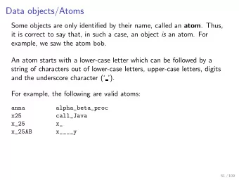
Single atom identification and manipulation using atomic force - PowerPoint PPT Presentation
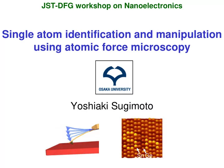
JST-DFG workshop on Nanoelectronics Single atom identification and manipulation using atomic force microscopy Yoshiaki Sugimoto Sn Ge Introduction Japan Osaka S. Morita M. Abe O. Custance Associate Professor Professor Visiting
JST-DFG workshop on Nanoelectronics Single atom identification and manipulation using atomic force microscopy Yoshiaki Sugimoto Sn Ge
Introduction Japan Osaka S. Morita M. Abe O. Custance Associate Professor Professor Visiting Associate Professor
Bottom-up nanotechnology The technology for atom- -by by- -atom construction of atom construction of nano nano- -devices devices The technology for atom 1959 1982 1959 1982 There's Plenty of There's Plenty of Invention of STM Invention of STM Logic gate constructed Logic gate constructed Room at the Bottom Room at the Bottom by atom manipulation by atom manipulation T=5 K CO molecule R.P. Feynman G. Binnig Binnig H. Rohrer R.P. Feynman G. H. Rohrer T=4 K Atom manipulation Atom manipulation Xe atom Cu(111) surface A.J. Heinrich, et al., Science Science 298 298 (2002) 1381. (2002) 1381. A.J. Heinrich, et al., Ni(100) surface D.M. Eigler Eigler, et al., , et al., Nature Nature 344 344 (1990) 524. (1990) 524. D.M.
Our approach Previous atom manipulation and assembly atom manipulation and assembly Previous At cryogenic temperature Using Scanning tunneling microscopy (STM) Our approach Our approach At room temperature At room temperature Evaporation of various atom species various atom species Using Atomic force microscopy (AFM) Using Atomic force microscopy (AFM) Atom Atom Atom Atom Identification Manipulation Identification Manipulation
Outline At room temperature Atom manipulation Using AFM Atom Atom identification discrimination Atom A B A A imaging A B A A
Atom imaging Atom At room temperature manipulation Atom Using AFM Atom identification discrimination Atom A B A A imaging A B A A
Experimental setup Top view Base pressure <5 × 10 -11 Torr Top view of AFM unit Side view Commercial Si cantilever (Nano World) f 0 =160 kHz, k=30 N/m, Q=13000, A=20 nm (Typical values) Ar ion sputtering ( UHV )
AFM images of various surfaces Si(111)-(7x7) Si(100)-(2x1) Ge(111)-c(2x8) Si atom Ge atom Si atom Semiconductor Pb/Si(111)-(1x1) KCl(100) Metal Insulator
Atom discrimination Atom At room temperature manipulation Atom Using AFM Atom identification discrimination Atom A B A A imaging A B A A
Discrimination between Sn and Si atoms Sn/Si(111)-( √ 3 × √ 3) Sn:50% Si:50% Sn:75% Si:25% Sn:99% Si:1% Si Sn The amount of evaporated Sn atoms increases Sn atoms Si surface
The limitation of atom discrimination from image In and Si Sn and Ge Sb and Si Si Sn In Si Sb Ge Si, Sn, and Pb mixed surface Only two More than three atomic contrasts? atomic contrasts?
Atom identification Atom At room temperature manipulation Atom Using AFM Atom identification discrimination Atom A B A A imaging A B A A
Atom identification based on force measurement Si, Sn, Pb mixed surface Sn Pb Si Si Si Si F Si-Si F Si-Sn F Si-Pb Si Sn Pb The chemical bonding force between tip apex atoms and surface atoms can be measured by AFM.
The method for measuring the interaction force The chemical bonding force between tip apex atoms and surface atoms can be measured. 0 3 3 -2 2 2 -4 A R = − H F -6 vdW 2 1 1 6 Z -8 -10 Δf[Hz] 0 0 F[nN] F[nN] -12 -14 -1 -1 Δ f -16 Numerical -2 -2 -18 F calculation -20 Total -3 -3 -22 F vdW f F ( z ) z -24 ∫ A Δ = − 0 f dz -4 -4 π 2 − − A k A 2 2 A z 0 2 4 6 8 10 12 14 16 18 20 22 24 0 0 2 2 4 4 6 6 8 8 10 12 14 16 18 20 22 24 10 12 14 16 18 20 22 24 Z[Å] Z[Å] Z[Å] NC-AFM Subtraction 3 2 1 0 F[nN] -1 F Short =F Total -F vdW -2 -3 -4 0 2 4 6 8 10 12 14 16 18 20 22 24 Z[Å]
The chemical bonding force: Sn and Si Sn 2 2 2 2 2 2 Sn n S 1 1 1 1 1 1 Si Si Si 0 0 0 0 0 0 F [nN] F [nN] F [nN] F [nN] F [nN] F [nN] F [ F [ F [ F [ F [ F [ -1 -1 -1 -1 -1 -1 -1 -1 -1 -1 -1 -1 Atom tracking technique -2 -2 -2 -2 -2 -2 -2 -2 -2 -2 -2 -2 -3 -3 -3 -3 -3 -3 -3 -3 -3 -3 -3 -3 -2 -2 -2 -2 -2 -2 -2 -2 -2 -2 -2 -2 -1 -1 -1 -1 -1 -1 -1 -1 -1 -1 -1 -1 0 0 0 0 0 0 1 1 1 1 1 1 2 2 2 2 2 2 3 3 3 3 3 3 Dist Distance [Å] Dist Dist Distance [Å] Distance [Å] Dist Distance [Å] Distance [Å] Dist Dist Distance [Å] ance [Å] ance [Å] ance [Å] ance [Å] ance [Å] e [Å] We repeated force measurements using different tip apex states. Lateral precision: ± 0.1Å Different cantilevers M. Abe, et al., Appl Appl. Phys. . Phys. Lett Lett. . M. Abe, et al., Different tip structure and composition 87 (2005) 173503. (2005) 173503. 87 by intentional tip-surface contact
Marked tip-apex dependence Sn/Si Pb/Si Sn/Si Pb/Si 0. 0.5 2 5 sets by various tip states 5 sets by various tip states 1 0.0 0. 0 -0.5 -0. F [nN] N] F [nN] N] F [ F [ -1 -1 -1.0 -1. Sn n Pb S Pb -2 -2 -1. -1.5 Si Si Si Si -3 -3 -2.0 -2. -2 -2 -1 -1 0 1 2 3 -1 -1 0 1 2 3 Dis Distance [Å ce [Å] ] Distan Distance ce [Å [Å] Absolute values of the chemical bonding force strongly depend on the tip apex structure or composition. Different force Absolute values of the chemical bonding force is useless for atom identification
Averaged relative interaction ratio Sn/Si Pb/Si Sn/Si Pb/Si 0. 0.5 2 5 sets by various tip states 5 sets by various tip states e l 1 0. 0.0 g n i s 0 -0. -0.5 e N] F [nN] F [nN] N] h t F [ r F [ o -1 -1 -1. -1.0 n f o s i t Sn n t Pb S Pb a n -2 -2 c -1.5 -1. i r i f p i Si Si r Si t Si n e -3 -3 g e -2. -2.0 d n -2 -2 -1 -1 0 1 2 i 3 -1 -1 0 1 2 3 i F m Dis Distance [Å ce [Å] ] Distan Distance ce [Å [Å] o t a 0. 0.8 1.0 1. Sn/Si relative relative Pb/Si relative Pb/Si relative Sn/Si 0. 0.6 0.8 0. 0.6 0. 0.4 0. interaction ratio: 77% interaction ratio: 59% interaction ratio: interaction ratio: 0.4 0. 0.2 0. et) et) (Set 0.2 0. (Set 0.0 0. Si ( Si ( F Si F Si 0. 0.0 F / F F / F -0. -0.2 F / F / -0. -0.2 -0.4 -0. -0. -0.4 -0. -0.6 -0. -0.6 -0. -0.8 -0.8 -0. -1. -1.0 -1.0 -1. -2 -1 0 0 1 1 2 2 3 3 -1 -1 0 1 2 3 Distance Distan ce [Å [Å] Distance Distan ce [Å [Å] The relative interaction ratio relative interaction ratio of the maximum attractive chemical bonding forces of the maximum attractive chemical bonding forces The for the same tip remains nearly constant independently on the tip remains nearly constant independently on the tip for the same tip
Atom fingerprints F Sn / F Si =0.77 F Pb / F Si =0.59 F Si F Sn F Pb Si Sn Pb F’ Sn / F’ Si =0.77 F’ Pb / F’ Si =0.59 F’ Si F’ Sn F’ Pb Si Sn Pb
Recommend
More recommend
Explore More Topics
Stay informed with curated content and fresh updates.
