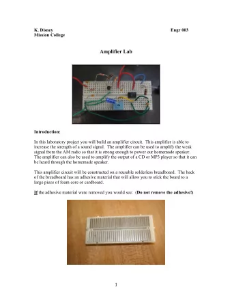
RF Power Amplifier Design Markus Mayer & Holger Arthaber - PowerPoint PPT Presentation
RF Power Amplifier Design Markus Mayer & Holger Arthaber Department of Electrical Measurements and Circuit Design Vienna University of Technology June 11, 2001 Contents Basic Amplifier Concepts Class A, B, C, F, hHCA Linearity
RF Power Amplifier Design Markus Mayer & Holger Arthaber Department of Electrical Measurements and Circuit Design Vienna University of Technology June 11, 2001
Contents � Basic Amplifier Concepts � Class A, B, C, F, hHCA � Linearity Aspects � Amplifier Example � Enhanced Amplifier Concepts � Feedback, Feedforward, ... � Predistortion � LINC, Doherty, EER, ... 2
Efficiency Definitions P η = OUT � Drain Efficiency: D P DC − − P P 1 � Power Added Efficiency: η = = η ⋅ OUT IN 1 PA D P G DC 3
Ideal FET Input and Output Characteristics I DS V =0 GS I m g m V =V GS P V GS V DS 2V P V P 0 0 V K V DD V DSmax Ohmic Saturation Breakdown − V V κ = DD K V DD 4
Maximum Output Power Match I DS V =0 GS I m g m V =V GS P V GS V DS 2V P V P 0 0 V K V DD V DSmax Ohmic Saturation Breakdown − V V = R DS max K OPT I m 5
Class A I DS I DS I m I m V GS V DS Q 2V P V P 0 0 V K V DD V DSmax 0 p 2 p V GS V DS p 2 p Q 6
Class A – Circuit V DD D G R L S η = κ ⋅ 50% D = G G (e.g. 14 dB) A η = κ ⋅ 48% PA 7
Class B I DS I DS I m I m V GS V DS Q 2V P V P 0 0 V K V DD V DSmax 0 p 2 p V GS V DS p 2 p Q 8
Class C I DS I DS I m I m V GS V DS Q 2V P V P 0 0 V K V DD V DSmax 0 p 2 p V GS V DS p 2 p Q 9
Class B and C – Circuit V DD f 0 D G R L S Class B Class C η = κ ⋅ η → 78 % 100 % D D = → G G - 6dB (8 dB) G 1 A η = κ ⋅ η PA → 0 % 65 % PA 10
Influence of Conduction Angle 11
Class F (HCA ... harmonic controlled amplifier ) I DS I DS I m I m V GS V DS Q 2V P V P 0 0 V K V DD V DSmax 0 p 2 p V GS V DS p 2 p Q 12
hHCA (half sinusoidally driven HCA) I DS I DS I m I m V GS V DS Q 2V P V P 0 0 V K V DD V DSmax 0 p 2 p V GS V DS p 2 p Q 13
Class F and hHCA – Circuit V DD Z o (n) 0, n=1 I D inf, n=odd Z e (n) V DS R L 0, n=even inf, n=even Class F hHCA η = κ ⋅ η = κ ⋅ 10 0% 10 0% D D = = + G G - 5dB (9 dB) G G 1dB (15 dB) A A η = κ ⋅ η = κ ⋅ 87 % 96 % PA PA 14
hHCA – Third Harmonic Peaking I DS I DS I m I m V GS V DS Q 2V P V P 0 0 V K V DD V DSmax 0 p 2 p V GS V DS p 2 p Q 15
Third Harmonic Peaking – Circuit V DD 3f 0 D G f 0 R L S η = κ ⋅ 91% D = + G G 0.6dB (14.6 dB) A η = κ ⋅ 87 % PA 16
Linearity Aspects 17
Linearity Aspects � Class A � Class AB � Class B � Class C 18
Linearity Aspects � Ideal strongly nonlinear model � Strong-weak nonlinear model 19
Amplifier Design – An Example � Balanced Amplifier Configuration Port 1 Z=50 Ohm Port 2 Z=50 Ohm 20
Amplifier Design – Simulation � Gate & Drain Waveforms Gate waveforms Drain waveforms 1 1000 25 5000 Inner Drain Voltage (L, V) Inner Drain Current (R, mA) Amp Amp 20 4000 0 500 15 3000 -1 0 10 2000 5 1000 -2 -500 0 0 Inner Gate Voltage (L, V) Inner Gate Current (R, mA) Amp Amp -3 -1000 -5 -1000 0 500 1000 1300 0 500 1000 1300 Time (ps) Time (ps) 21
Amplifier Design – Simulation � Dynamic Load Line & Power Sweep Dynamic load line Power Sweep 1 Tone 8000 40 80 IVCurve (mA) Output Power (L, dBm) IV_Curve 70 Amp 6000 Dynamic Load Line (mA) PAE (R) 30 60 Amp Amp 50 4000 20 40 2000 30 10 20 0 10 -2000 0 0 0 3 6 9 12 15 0 5 10 15 20 24 Voltage (V) Power (dBm) 22
Amplifier Design – Measurements � Single Tone & Two Tone 60 60 P A E [% ] 4 0 8 0 P A E [% ] 1 d B C P 3 5 7 0 50 50 3 0 6 0 P out [dBm], IMDD [dBc], Gain [dB] 40 40 P out [dBm], Gain [dB] 2 5 5 0 P out P o u t IM D D G a in 30 30 2 0 4 0 G ain G a m m a In P A E P A E 1 5 3 0 20 20 1 0 2 0 10 10 5 1 0 0 0 0 0 0 5 1 0 1 5 2 0 2 5 3 0 3 5 0 5 10 15 20 25 30 35 P in [d B m ] P in [dB m ] 23
Amplifier Nonlinearity � Gain and Phase depends on Input Signal � 3 rd Order Gain-Nonlinearities: 24
Amplifier Nonlinearity � Higher Output Level (close to Saturation) results in more Distortion/Nonlinearity 25
Nonlinearity leads to? � Generation of Harmonics � Intermodulation Distortion / Spectral Regrowth � SNR (NPR) Degradation � Constellation Deformation 26
Intermodulation and Harmonics 27
Spectral Regrowth 10 ACPR 1 >60dB ACPR 2 >60dB 0 ACPR 1 =16dB ACPR 2 =43dB -10 relative power / dB -20 -30 -40 -50 -60 -15 -10 -5 0 5 10 15 relative frequency / MHz � Energy in adjacent Channels � ACPR (Adjacent Channel Leakage Power Ratio) increases 28
Reduced NPR (Noise Power Ratio) � Input Signal � Output Signal of Nonlinear Amplifier � Degradation of Inband SNR � „Noisy“ Constellation 29
Constellation Deformation � Input Signal � Output Signal of Nonlinear Amplifier (with Gain- and Phase-Distortion) 30
Modeling of Nonlinearities � with Memory-Effects � Volterra Series (=„Taylor Series with Memory“) � without Memory-Effects α α 2 r r performance = = Θ � Saleh Model a f ( r ) g ( r ) + β + β 2 2 1 r 1 r better Θ a � Taylor Series � Blum and Jeruchim Model � AM/AM- and AM/PM-conversion 31
AM/AM- and AM/PM-Conversion � GaAs-PA 32
AM/AM- and AM/PM-Conversion � LDMOS-PA 33
How to preserve Linearity? � Backed-Off Operation of PA � Simplest Way to achieve Linearity � Linearity improving Concepts � Predistortion � Feedforward � ... 34
How to preserve Efficiency? � Efficiency improving Concepts � Doherty � Envelope Elimination and Restoration � ... � Linearity improving Concepts � Higher Linearity at constant Efficiency � Higher Efficiency at constant Linearity 35
Direct (RF) Feedback � Classical Method � Decrease of Gain � Low Efficiency � Feedback needs more Bandwidth than Signal � Stability Problems at high Bandwidths 36
Distortion Feedback � Feedback of outband Products only � Higher Gain than RF feedback � Stability Problems due to Reverse Loop 37
Feedforward � Overcomes Stability Problem by forward-only Loops � Critical to Gain/Phase-Imbalances 0.5dB Gain Error � -31dB Cancellation 2.5° Phase Error � -27dB Cancellation � Well suited for narrowband application 38
Cartesian Feedback baseband input I modulator main amp. I RF-output OPAs Q Q local UMTS example : oscillator 10 original signal I predistorted signal 0 Q demodulator -10 relative power / dB -20 � AM/AM- and -30 AM/PM-correction -40 � High Feedback-Bandwidth -50 � Stability Problems -60 -30 -20 -10 0 10 20 30 relative frequency / MHz 39
Digital Predistortion � Digital Implementation of „Cartesian Feedback“ � Additional ADCs, DSP Power, Oversampling needed � Loop can be opened � no Stability Problems 40
Analog Predistortion � Predistorter has inverse Function of Amplifier � Leads to infinite Bandwidth (!) � Hard to realize (accuracy) 41
Analog Predistortion � Possible Realizations: 42
LINC (Linear Amplification by Nonlinear Components) s (t) Ks (t) 1 1 K K(s (t)+ s (t)) 1 2 signal s(t) =Ks(t) separation s (t) Ks (t) 2 2 K UMTS example : 10 � AM/AM- and ACPR 1 >60dB s(t) ACPR 2 >60dB AM/PM-correction 0 s 1 (t) ACPR 1 =18dB ACPR 2 =29dB � Digital separation required -10 relative power / dB (accuracy!) -20 � High Bandwidth, -30 oversampling necessary -40 � Stability guaranteed -50 -60 -30 -20 -10 0 10 20 30 relative frequency / MHz 43
Doherty Amplifier � Auxiliary amplifier supports main amplifier during saturation � PAE can be kept high over a 6dB range 44
Doherty Amplifier � Gain vs. Input Power � Efficiency vs. Input Power P OUT doherty configuration (A1+A2) main amp. (A1) aux. amp. (A2) P IN � No improvement of AM/AM- and AM/PM-distortion � Behavior of auxiliary amplifier very hard (impossible) to realize � Stability guaranteed 45
EER (Envelope Elimination and Restoration) � Separating phase and magnitude information � Elimination of AM/AM-distortion � Application of high-efficient amplifiers (independent of amplitude distortion) � Stability guaranteed amplitude information RF input signal separation phase information RF output high efficiency power amplifier 46
EER (Envelope Elimination and Restoration) supply voltage � Analog realization peak detector amplifier � Limiter hard to build � Accuracy problems limiter � Feedback necessary RF input RF output high efficiency peak detector power amplifier � Digital realization � Oversampling + high D/A- amplitude information conversion rates required supply voltage amplifier D digital baseband input � High power consumption A I of DSP and D/A-converters digital D modulator signal � Possible feedback A Q I RF output processor Q elimination D high efficiency � Compensation of AM/PM- A power amplifier phase information distortion possible local oscillator 47
Recommend
More recommend
Explore More Topics
Stay informed with curated content and fresh updates.
