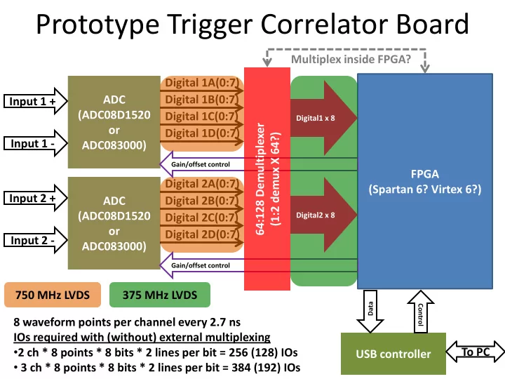

Prototype Trigger Correlator Board Multiplex inside FPGA? Digital 1A(0:7) Digital 1B(0:7) ADC Input 1 + (ADC08D1520 Digital 1C(0:7) Digital1 x 8 64:128 Demultiplexer or Digital 1D(0:7) (1:2 demux X 64?) Input 1 - ADC083000) Gain/offset control FPGA Digital 2A(0:7) (Spartan 6? Virtex 6?) Input 2 + Digital 2B(0:7) ADC (ADC08D1520 Digital 2C(0:7) Digital2 x 8 or Digital 2D(0:7) Input 2 - ADC083000) Gain/offset control 750 MHz LVDS 375 MHz LVDS Data Control 8 waveform points per channel every 2.7 ns IOs required with (without) external multiplexing • 2 ch * 8 points * 8 bits * 2 lines per bit = 256 (128) IOs To PC USB controller • 3 ch * 8 points * 8 bits * 2 lines per bit = 384 (192) IOs
Specification Required Value ADC08D1520 ADC083000 ADC sampling rate >= 2.6 GSa/s 1.5 (2ch) / 3.0 GSa/s (1ch) 3.0 GSa/s Analog Bandwidth >~700 MHz 2 GHz “full power BW” 3 GHz “full power BW” Nominal range ?? 650 mV or 870 mV 600 mV or 820 mV Adjustable range Preferred +/- 20% full scale 560 mV – 840 mV Adjustable offset Preferred +/- 45 mV +/- 45 mV ADC digital output Streaming 4x750MHz LVDS per bit 4x750MHz LVDS* ADC bits >= 3 8 8 Total channels >= 2 2 (1.5 GSa/s) / 1 (3.0 GSa/s) 1 Differential input Preferred Yes Yes Power 1.6 W per 3.0 GSa/s channel 1.9 W per channel Est. cost / unit $613 per channel $686 per channel Clock required 1.5 GHz differential 1.5 GHz differential I prefer the slightly cheaper ADC since we could also use it to add 2 more channels (at a lower sampling rate) to see how the FPGA code holds up with more inputs. FPGA choice probably should wait until someone has a rough VHDL implementation of algorithm so we see what resources are required.
ASIC for 3 Bit Continuous Digitizing
Recommend
More recommend