Performance Enhancement of P-channel InGaAs Quantum-well FETs by - PowerPoint PPT Presentation
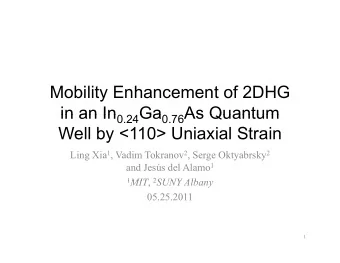
Performance Enhancement of P-channel InGaAs Quantum-well FETs by Superposition of Process-induced Uniaxial Strain and Epitaxially-grown Biaxial Strain Ling Xia 1 , Vadim Tokranov 2 , Serge R. Oktyabrsky 2 , and Jess A. del Alamo 1 1
Performance Enhancement of P-channel InGaAs Quantum-well FETs by Superposition of Process-induced Uniaxial Strain and Epitaxially-grown Biaxial Strain Ling Xia 1 , Vadim Tokranov 2 , Serge R. Oktyabrsky 2 , and Jesús A. del Alamo 1 1 Microsystems Technology Laboratories, MIT, USA; 2 College of Nanoscale Science and Engineering, SUNY-Albany, USA. Dec. 06, 2011 Sponsors: Intel Corp. and FCRP-MSD Center. Fabrication: MTL at MIT.
Outline • Motivation • Mechanical simulations • Device technology • Experimental results • Conclusions 2
Motivation • Interests in InGaAs CMOS – Fueled by excellent v e and µ e • Key challenge for InGaAs CMOS • Bridging performance gap between n- and p-FET. • Our approach – Introduce strain to InGaAs p-FET • Uniaxial + biaxial compressive strain Logarithmic scale Electron mobility Hole mobility Kuhn, IWJT, 2010 del Alamo, Nature, 2011 3
Why biaxial strain + uniaxial strain? • Sources for strain include: – Epitaxial lattice mismatch Biaxial strain – Fabrication process Uniaxial strain π <110> = ‐Δ µ /( µ 0 σ <110> ) Max <110> piezoresistance coefficient 120 In 0.24 Ga 0.76 As 100 2 /dyn) 80 Ge GaAs 60 12 cm Gomez, EDL, 2010 40 (10 Weber, IEDM, 2007 Xia, TED, 2011 20 Experiments Xia, ISCS, 2011 0 -2.5 -2.0 -1.5 -1.0 -0.5 0.0 Epitaxial compressive biaxial strain (%) • Enhancements of µ h by biaxial and uniaxial strain add superlinearly • Similar effect found in Si simulations (Wang, TED, 2006) 4
InGaAs QW-FET with uniaxial + biaxial strain • Self-aligned stressor (compressively stressed) • Self-aligned metal layer (Mo) • Carbon delta-doping • Biaxial strain in the channel as grown • Induced stress scalable with L G (next slide) 5
Mechanical stress simulations • Parameters used in simulations: t SiN = 200 nm; SiN σ int = -2 GPa Longitudinal stress distribution L G = 2 µm t SiN =200 nm S L side = 100 nm D Cut line -1 0 x (µm) • Desirable stress type can be obtained with the proposed stressor structure • Compressive longitudinal stress µ h ↑ • Tensile transverse stress µ h ↑ 6
L G scalability of induced stress at middle of gate Projected assuming Δ µ h / µ h = - π · σ 180% 300 π // = - 1.2x10 -10 cm 2 /dyn π = 0.7x10 -10 cm 2 /dyn 0 150% Fast increase (Xia, ISCS, 2011) Stress (MPa) -300 when L G ~ t SiN 120% Slow increase Δ µ h / µ h0 -600 when L G >> t SiN Slow down 90% σ // From due to a σ -900 fixed L side From 60% Longitudinal Total Transverse -1,200 30% -1,500 10 100 1,000 10,000 0% 10 100 1000 10000 L G (nm) L G (nm) • L G ↓ Stress ↑ inside gate opening • Assume linear ∆ µ with σ >160% µ h enhancement for L G < 50 nm 7
Device technology SiO 2 SiO 2 SiN SiN Mesa isolation D D S S Ohmic metalization Mo Mo Cap : 2x10 19 cm -3 Cap : 2x10 19 cm -3 Carbon doped GaAs Carbon doped GaAs Molybdenum (Mo) deposition Al 0.42 Ga 0.58 As Al 0.42 Ga 0.58 As Barrier Barrier In 0.24 Ga 0.76 As In 0.24 Ga 0.76 As Channel Channel PECVD SiN stressor and SiO 2 AlGaAs AlGaAs Buffer Buffer Anisotropic ECR RIE SiO 2 /SiN SiO 2 SiO 2 SiO 2 SiO 2 Anisotropic ECR RIE Mo SiN SiN Isotropic RIE Mo S D S D G Mo Mo GaAs cap recess by wet etching Cap : 2x10 19 cm -3 Cap GaAs Cap : 2x10 19 cm -3 Cap Carbon doped GaAs Carbon doped GaAs Gate metalization Al 0.42 Ga 0.58 As Barrier Al 0.42 Ga 0.58 As Barrier In 0.24 Ga 0.76 As Channel Channel In 0.24 Ga 0.76 As AlGaAs AlGaAs Buffer Buffer Key considerations: • Avoid Mo layer short to gate metal • Air gap as small as possible 8
Device cross-section Artifact of imaging • L G = 2 µm; channel along [-110] • L side 400 nm 9
Experimental parameters for devices •Split experiments: • SiN with -2.1 GPa stress vs SiN with 0 Pa stress • SiN film stress obtained from wafer curvature measurements • L G = 2 µm to 8 µm • Four channel orientations: S D S D G [-110] G [110] [-110] [110] [100] [010] 10
QW-FET electrical characteristics • Example: L G = 2 µm; channel along [-110] 40 10 0 GPa SiN -2.1 GPa SiN V GS - V T = -0.75 V -2 GPa SiN 0 GPa SiN 8 30 | g m | (mS/mm) -I D (mA/mm) Intrinsic 6 -0.55 V 20 V DS = -2 V 4 -0.35 V 10 Extrinsic 2 -0.15 V 0 0 -0.5 0 0.5 -2.0 -1.5 -1.0 -0.5 0.0 V GS - V T (V) V DS (V) • Significant drive current increase • Transconductance increase at all gate overdrives 11
Subthreshold characteristics and V T • Similar I G as chemically etched samples No RIE damage • V T shift between high- and low- stress samples – Likely due to different anisotropic RIE overetch With -2 GPa SiN 10 With 0 GPa SiN 1 I D | I | (mA/mm) 0.1 Both S = 103 mV/dec 0.01 I G 1E-3 1E-4 L G = 2 m V DS = -2 V 1E-5 -0.8 -0.6 -0.4 -0.2 0.0 0.2 0.4 0.6 0.8 1.0 V GS (V) 12
L G dependence of g m 30 V DS = -2 V 25 V GS – V T = -0.5 V | g m-sat | (mS/mm) +36% 20 15 10 Dots : data Lines: least-square fittings 5 Channel along [-110] 0 2 4 6 8 L G ( m) • Increasing enhancement observed with decreasing L G • Consistent with stress simulations + π measurements >160% enhancement expected with L G < 50 nm 13
Crystal direction dependence g mi_sat • Observed anisotropic ∆ g mi and ∆ R SD – g mi extracted using g mext , R S , R D and g D – R S , R D extracted using gate current injection method • <110> anisotropy consistent with measurements of piezoresistance coefficients – π [-110] : π [110] = 2.6 (Xia, ISCS, 2011) 14
Theoretical discussions • Valence band change due to strain in InGaAs – Used k.p methods (nextnano 3 ) – Calculated subbands in In 0.24 Ga 0.76 As quantum well 0.1 No uniaxial -0.06 0.08 -500 MPa uniaxial hh1 [-110] uniaxial 0.06 m * ↑ -0.08 m * // ↓ 0.04 0.02 k y (2 / a) -0.1 E v (eV) lh1 0 No uniaxial -0.02 -0.12 -0.04 -0.06 -0.14 -0.08 hh2 [010] [110] -0.1 -0.1 -0.05 0 0.05 0.1 -0.16 k x (2 / a) -0.1 -0.05 0 0.05 0.1 k [110] k //[-110] In-plane iso-energy [100] • Compressive strain parallel to contours of hh1 with and channel is desirable without uniaxial strain 15
Effective mass model • Treat nonparabolic valence band using energy dependent m * (De Michielis, TED, 2007) [-110] Strain Gate Barrier P z (z) Channel -0.06 [-110] uniaxial m * ↑ m * // ↓ -0.08 [110] uniaxial -0.1 No uniaxial E v (eV) -0.12 -0.14 -0.16 -0.1 -0.05 0 0.05 0.1 k <110> k //<110> From simulations: • ∆ m * anisotropy induced by quantization change due to piezoelectric effect • ∆ m * anisotropy consistent with g m measurements.
Conclusions • Developed device architecture for InGaAs p-FETs that incorporates uniaxial strain through self-aligned dielectric stressor • Key results: – Biaxial strain + uniaxial strain substantial enhancements in transport characteristics – Up to +36% ∆ g m observed in L G = 2 µm device – Strong enhancement anisotropy due to piezoelectric effect • For further enhancement: – Scale down L G and bring S/D closer – Project ∆ g m >160% @ L G < 50 nm • Study useful to other p-type III-V materials (e.g. InGaSb, InSb) 17
Recommend
More recommend
Explore More Topics
Stay informed with curated content and fresh updates.
