Overview Homework Circuit Timing Introduction to Structured VLSI - PowerPoint PPT Presentation
Overview Homework Circuit Timing Introduction to Structured VLSI Design Controller Datapath Control Structures Dependency Graph Precedency Graph VHDL Presentation of Assignment 2 Joachim Rodrigues Joachim Rodrigues,
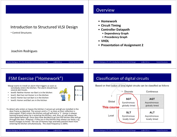
Overview • Homework • Circuit Timing Introduction to Structured VLSI Design • Controller Datapath ‐ Control Structures • Dependency Graph • Precedency Graph • VHDL • Presentation of Assignment 2 Joachim Rodrigues Joachim Rodrigues, EIT, LTH, Introduction to Structured VLSI Design jrs@eit.lth.se Control Structures Joachim Rodrigues, EIT, LTH, Introduction to Structured VLSI Design jrs@eit.lth.se Control Structures FSM Exercise (”Homework”) Classification of digital circuits Marge wants to install an alarm that triggers as soon as somebody enters the kitchen. The alarm should have several alert levels. • level0: Neither Homer nor Bart is in the kitchen • level1: Bart but not Homer is in the kitchen • level2: Homer but not Bart is in the kitchen • level3: Homer and Bart are in the kitchen This course To detect who enters or leaves the kitchen 2 sensors g1 and g0 are installed in the door frame as depicted. The sensors emit a ‘1’ as soon as their reflection is interrupted. If Bart enters the kitchen only g0 will emit a ‘1’. Homer is always leaning forward when he is entering the kitchen, and, thus, g1 will always be interrupted before g0. Once they have decided to go into the kitchen they will go through the door. However, if they are in the kitchen they always can leave, e.g., level3 changes to level2. The size of Homers hips and belly prevent them from entering the kitchen simultaneously. The clock frequency is 1MHz. Joachim Rodrigues, EIT, LTH, Introduction to Structured VLSI Design jrs@eit.lth.se Control Structures Joachim Rodrigues, EIT, LTH, Introduction to Structured VLSI Design jrs@eit.lth.se Control Structures
Classification Classification, schematical • SGT (synchronous globally timed): SGT SLT – Global clock, r s Discrete time – Fixed module latencies, One BIG FSM FSM1+ FSM2+ FSM + datapath r f • SLT (synchronous locally timed): datapath1 datapath2 clk clk – Global clock, Hierarchy of (local) FSMs – Variable module latencies (start ‐ & finish signals) • ALT (asynchronous locally timed): GALS (globally asynchronous locally synch. (ALT) GALS (ALT) All asynchronous – Local clocks Contineous r s r s – Synchronization + protocol at interfaces s FSM2'+ FSM1'+ s Control1”+ Control2”+ All asynchronous: time r f r f datapath1 ' datapath2 ' datapath1 ” datapath2” – Handshake components clk1 clk2 – Channels (data+req+ack) everywhere • AGT (asynchronous globally timed): s = Synchronizer Data connections not shown Nonsense 6 Joachim Rodrigues, EIT, LTH, Introduction to Structured VLSI Design jrs@eit.lth.se Control Structures Joachim Rodrigues, EIT, LTH, Introduction to Structured VLSI Design jrs@eit.lth.se Control Structures Combinatorial Circuit Datapath = r ( x ) p ( g ( f ( x )), p ( f ( x ), h ( x ))) A EN B EN B A CLK CLK r ( x ) g f x x r ( x ) p 2 g p h f p h 1 f D h D p D x D g D • Expensive (no reuse of operator modules) • Not flexible (fixed function) Tri ‐ state • Modules idle for large periods of time buffer Controlled by drivers and register enable signals. • P1 and P2 realize the same function What do we need to do if we want to reuse p? Controller+ DP Joachim Rodrigues, EIT, LTH, Introduction to Structured VLSI Design jrs@eit.lth.se Control Structures Joachim Rodrigues, EIT, LTH, Introduction to Structured VLSI Design jrs@eit.lth.se Control Structures
SGT module: FSM + Data path SLT module: FSM + Datapath Start and finish signals. CLK CLK Local FSMs inside modules. Hierarchy of FSMs Enables modular design In principle: FSM FSM r S One global controller ! r F Control signals from previous x D f D g D h D A EN B EN x D f D g D h D A EN B EN p D p D slide x x r ( x ) r ( x ) DataPath DataPath Joachim Rodrigues, EIT, LTH, Introduction to Structured VLSI Design jrs@eit.lth.se Control Structures Joachim Rodrigues, EIT, LTH, Introduction to Structured VLSI Design jrs@eit.lth.se Control Structures SLT ‐ module Interface SLT ‐ module Interface CLK CLK r S r F x r ( x ) FSM r S r F CLK x D f D g D h D p D A EN B EN r S x x r ( x ) DataPath r F r ( x ) Joachim Rodrigues, EIT, LTH, Introduction to Structured VLSI Design jrs@eit.lth.se Control Structures Joachim Rodrigues, EIT, LTH, Introduction to Structured VLSI Design jrs@eit.lth.se Control Structures
The Recipe Combinatorial Circuit = Dependency Graph = 1. Given a data ‐ path r ( x ) p ( g ( f ( x )), p ( f ( x ), h ( x ))) 2. Identify precedence constraints inherent in expression (data dependency graph) Essential precedence constraints g f x 3. Identify precedence constraints imposed by: r ( x ) – Data ‐ path topology non ‐ essential constraints – Components essential constraints h p p 2 1 4. Precedence graph with – Register loads – All precedence constraints output of each operation needs to secured in a register 5. Design the FSM Joachim Rodrigues, EIT, LTH, Introduction to Structured VLSI Design jrs@eit.lth.se Control Structures Joachim Rodrigues, EIT, LTH, Introduction to Structured VLSI Design jrs@eit.lth.se Control Structures Final Precedence Graph Final Precedence Graph = = r ( x ) p ( g ( f ( x )), p ( f ( x ), h ( x ))) r ( x ) p ( g ( f ( x )), p ( f ( x ), h ( x ))) 5 2 3 4 A holds input for g, hence f → A 1 g g g → f → g → f f x f → A x A A A r ( x ) r ( x ) x → x → 6 A A h p p → h p p → p p h → p → B h → p → B B B B B 1 2 1 2 1 1 Only one bus: f → A and h → B in 2 cycles Why p 1 → B before g → A? Total: 6 clock cycles Because p takes inputs from both A and B. If we do g → A first p sees new inputs !! One datapath: Only one register can be loaded during one clock cycle!! Joachim Rodrigues, EIT, LTH, Introduction to Structured VLSI Design jrs@eit.lth.se Control Structures Joachim Rodrigues, EIT, LTH, Introduction to Structured VLSI Design jrs@eit.lth.se Control Structures
Improved Datapath Precedence Graph (improved DP) = r ( x ) p ( g ( f ( x )), p ( f ( x ), h ( x ))) B EN A EN B A CLK CLK r ( x ) x g f A ← A ← f g x ← A x r ( x ) g p h ← f B x h D B ← f D p D h p p x D g D B ← B ← p h p 2 1 1 Same as before:except: No required ordering of B ← f and A ← f x is loaded into B But still only one bus. Difference: operation h is driven by register B Joachim Rodrigues, EIT, LTH, Introduction to Structured VLSI Design jrs@eit.lth.se Control Structures Joachim Rodrigues, EIT, LTH, Introduction to Structured VLSI Design jrs@eit.lth.se Control Structures Improved Datapath Improved Datapath f g A ← A ← f g f g A ← A ← f g ← A x r ( x ) ← A x r ( x ) ← B x ← B x h B ← p p B ← h B ← p B ← p h B ← p B ← p p 1 1 2 h p 1 1 2 B EN B EN A EN A EN B B A A CLK CLK CLK CLK r ( x r ( x x x g p g h p h f f h D f D p D h D x D g D f D p D x D g D 2 nd cycle: h → B 1 st cycle: x → A,B Joachim Rodrigues, EIT, LTH, Introduction to Structured VLSI Design jrs@eit.lth.se Control Structures Joachim Rodrigues, EIT, LTH, Introduction to Structured VLSI Design jrs@eit.lth.se Control Structures
Improved Datapath Improved Datapath f g A ← A ← Now: T CL >T CLK f g x ← A x r ( x ) ← B x B EN A EN h p p B ← B B ← B ← p A h p 1 2 1 CLK CLK r ( x ) B EN A EN x B A CLK CLK 2 5 3 4 r ( x x g p h f h D f D p D x D g D g p h f h D f D p D x D g D Propagation delays in time units 3 rd cycle: f → A Joachim Rodrigues, EIT, LTH, Introduction to Structured VLSI Design jrs@eit.lth.se Control Structures Joachim Rodrigues, EIT, LTH, Introduction to Structured VLSI Design jrs@eit.lth.se Control Structures Precedence Graph (improved DP) Using a SLT controller 5 2 • What if g –module with latency = 2 cycles becomes A ← A ← f g g x f available? ← A x r ( x ) • Redesign and reimplement the FSM � ← B x 3 3 4 • If FSM: – responds to g S ‐ signal p B ← h p B ← B ← p h p 1 2 1 – produces gF ‐ signal and A f A then optimization of g –module is possible without any change of the FSM. B h B • This is SLT ‐ design g A • Still need to distribute zero ‐ skew clock to p1 B p2 B everywhere. 11 0 1 4 5 6 7 8 9 10 12 13 2 3 14 15 Joachim Rodrigues, EIT, LTH, Introduction to Structured VLSI Design jrs@eit.lth.se Control Structures Joachim Rodrigues, EIT, LTH, Introduction to Structured VLSI Design jrs@eit.lth.se Control Structures
Making an SLT module Making an SLT module CLK B EN A EN B A CLK CLK FSM r ( x ) r S r F x gS gF g p h gS f x D f D g D h D A EN B EN p D gF h D f D p D x D g D x r ( x ) DataPath Joachim Rodrigues, EIT, LTH, Introduction to Structured VLSI Design jrs@eit.lth.se Control Structures Joachim Rodrigues, EIT, LTH, Introduction to Structured VLSI Design jrs@eit.lth.se Control Structures SLT ‐ module Interface SLT ‐ module interface CLK CLK x S r F x r ( x ) FSM r S r F CLK x D f D g D h D p D A EN B EN x S x x r ( x ) DataPath r F r ( x ) Joachim Rodrigues, EIT, LTH, Introduction to Structured VLSI Design jrs@eit.lth.se Control Structures Joachim Rodrigues, EIT, LTH, Introduction to Structured VLSI Design jrs@eit.lth.se Control Structures
Recommend
More recommend
Explore More Topics
Stay informed with curated content and fresh updates.
