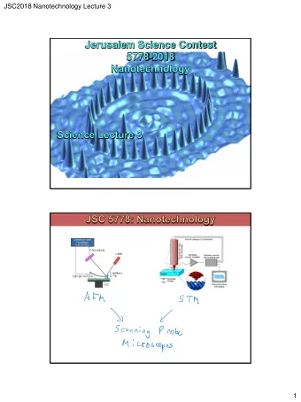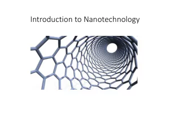
Nanotechnology Plasma & Nanotechnology Graphene nanoflakes - PowerPoint PPT Presentation
Nanotechnology Plasma & Nanotechnology Graphene nanoflakes CNT Si nanofibers Au nanodots Nano-Patterns Good and fast Start References : PRINCIPLES OF PLASMA DISCHARGES AND MATERIALS PROCESSING, MICHAEL A. LIEBERMAN & ALLAN
Nanotechnology
Plasma & Nanotechnology Graphene nanoflakes CNT Si nanofibers Au nanodots
Nano-Patterns
Good and fast Start ▪ References : ▪ PRINCIPLES OF PLASMA DISCHARGES AND MATERIALS PROCESSING, MICHAEL A. LIEBERMAN & ALLAN J. LICHTENBERG, John Wiley & Sons, Inc (2005). ▪ PHYSICS OF RADIO-FREQUENCY PLASMAS, PASCAL CHABERT & NICHOLAS BRAITHWAITE, Cambridge University Press (2011). ▪ Spacial issue „ Plasma and Nanotechnology“ : , J. Phys. D: Appl. Phys. 44 (2011)
Plasma ball
Low Temperature Plasma ▪ Low degree of ionization ▪ Neutral background the ion and electron density ▪ Collisions with the background gas is dominant compared to electron ion collisions ▪ Non-equilibrium plasmas at low pressures
Various applications
Plasma cleaning
Is it really hot? Does the ocean water temp. change?
Plasma Chemistry I ▪ Dissociation of feedstock gas into active neutral free radicals: ▪ Dissociation of the free radicals
Plasma Chemistry II ▪ Dissociative ionization and attachment: ▪ Chlorine discharge
Plasma Chemistry III ▪ Chemical reactions between neutrals in the presence of a third body ▪ ▪ At the substrate ▪ Removing ▪ Etching ▪ Deposition or growth
Plasma Etching ▪ An etched profile with ▪ 0.5 micrometer (500 Nanometer) wide ▪ 4 micrometer (4000 nanometer) ▪ Such profiles are used for device isolation and charge storage capacitores. ▪ Human hair is 50-100 micrometer in diameter.
Plasma Etching steps I a) Metal Deposition b) Photoresist deposition c) Optical exposure through a pattern d) Photoresist development
Plasma Etching steps II e) Anisotropic f) Photoresist etching removal ▪ Process Selectivity: ▪ Depends on the plasma species ▪ Energy threshold & energy activation
Wet and Dry etching ▪ Carbon Floride (CF4) does not react with Silicin (Si). ▪ Dissociative ionization and attachment: ▪ Wet etching + toward the Silicon substrate ▪ Dry etching: Accelerate CF 3
Plasma Etching steps II Wet etching Dry etching Chemical etching
Ion enhanced plasma etching
New world of integrated circuits?
New world of integrated circuits? Deposit or grow Oxygen & Argon Plasma: Deposition of SiO 2 on Si Deposition of Aluminum, Tungsten, superconducting films SiH 2 Cl 2 /NH 3 & Si(OC 2 H 5 ) 4 /O 2 Plasma: Deposition of Si 3 N 3 and SiO 2
New world of integrated circuits? Doping and modification BF3 discharge: Implant dopant B atoms into Silicon
New world of integrated circuits? Etching and removing CF4/Cl2/O2 discharges: Selectively remove silicon films O2 discharge: Remove photoresist and polymer films
Devices ▪ Capacitive coupled plasma are used in plasma etching and deposition process for production of: ▪ Integrated circuits ▪ Sollar cells Plasma electronics, Applications in Microelectronic Device Fabrication
Capacitive coupled plasma
Symmetric discharge ▪ The ion flux and the ion energies increase (decreases) by increasing (decreasing) the deriving frequency.
CCPs & blocking a Capacitor
Geometrically Asymmetric ▪ The RF current is constant. ▪ But the ground electroge Area is greater then the powered electrode area. ▪ The blocking capacitor blocks DC currents:
Particle and Potential distribution
Electrically Asymmetric ▪ The high frequency controls the ion plasma bulk (ion flux). ▪ The lower frequency controls the plasma sheath. ▪ The phase shift between the two sources controls also the sheath potential. ▪ The independent control is not always perfect.
Magnetron
Magnetic Asymmetry
High density sources (ICP)
High density sources (ECR)
Typical CCP parameters What are optimum plasma etching parameters?
The anistropy of the etching profile 2 Θ where 2 Θ is the angle of view : tan ( Θ )=D/2H • The etching profile is mainly determined by the ion flux, the ion energy, and the ion angular distribution. • High aspect ratio could be achieved employing narrower ion angular distribution. H • Assuming an etching profile as a hole, the aspect ratio is the ratio of the height of the hole to the diameter of the hole; 0.07 AR=H/D. 0.06 IAD [# m^-2 s^-1 deg^-1] 0.05 ▪ The direct ion heat flux hits the bottom of the 0.04 contact is given by 0.03 0.02 0.01 0.00 0.0 0.5 1.0 1.5 2.0 2.5 3.0 3.5 4.0 4.5 5.0 Angle [deg ] D ▪ The direct ion heat flux which a combination of the angular distribution and the ion energy Contact Hole distribution is given as
Sheath potential (I) ◼ Increasing the sheath potential increases the ion drift velocity normal to the electrode with respect to the ion velocity components parallel to the electrode, the result the angle of the maximum ion flux shifts toward zero. ◼ Sinsolidal electrode potential
Sheath potential (II) ◼ Increasing the sheath potential increases the ion drift velocity normal to the electrode with respect to the ion velocity components parallel to the electrode, the result the angle of the maximum ion flux shifts toward zero. ◼ Sinsolidal electrode potential
Ion Flux (I) ◼ Because it is really difficult to interpret the results of numerical models, it is necessary sometimes to use simple analytical models or available measurements. ◼ Lieberman’s model (*) is restricted to high frequency regime, however, it predicts that the high ion fluxes enter the sheath leads to thinner sheaths. ◼ This qualitatively agree with the simulation results. ◼ Back to the simulation results, Higher ion fluxes leads to thinner sheaths, narrower IAD, higher Direct ion flux and ion heat flux. *M.A. Liebermann, IEEE, 16 (1988) 638 equation(27).
Ion Flux (II) ◼ Because it is really difficult to interpret the results of numerical models, it is necessary sometimes to use simple analytical models or available measurements. ◼ Lieberman’s model (*) is restricted to high frequency regime, however, it predicts that the high ion fluxes enter the sheath leads to thinner sheaths. ◼ This qualitatively agree with the simulation results. ◼ Back to the simulation results, Higher ion fluxes leads to thinner sheaths, narrower IAD, higher Direct ion flux and ion heat flux. *M.A. Liebermann, IEEE, 16 (1988) 638 equation(27).
Gas Pressure (I) ◼ Increasing the background gas pressure broads the IADs. ◼ The scatter of ions decreases the direct ion flux and the direct ion heat flux at all aspect ratios.
Gas Pressure (I) ◼ Increasing the background gas pressure broads the IADs. ◼ The scatter of ions decreases the direct ion flux and the direct ion heat flux at all aspect ratios.
Direct Ion heat flux ◼ Direct ion heat flux at the bottom of a profile with dimensions : – depth of 100 nm. – Width of 5 nm.
Aluminum Oxide Deposition I
Aluminum Oxide Deposition II
Graphene ▪ It is a single layer of Carbon atoms arranged i a hexagonal lattice ▪ Zero band gap material ▪ The strongest material: 200 times steel ▪ Conducts heat and electricity effeciently ▪ Transparent ▪ Nonlinear diamagnetism
Graphene applications Computer chip Unbreakable faster 10000 than smart phones normal chip Batteries and super Low cost solar capacitors cells Storage more energy Charge faster Bone Tissue engineering Drug delivery Remove radioactive materials from water
Carbone nanotube
Carbone nanotube
Thanks!
Recommend
More recommend
Explore More Topics
Stay informed with curated content and fresh updates.
