MODEL ON A 32-BIT MICROCONTROLLER Nicolas Moro 1,3 , Amine Dehbaoui - PowerPoint PPT Presentation
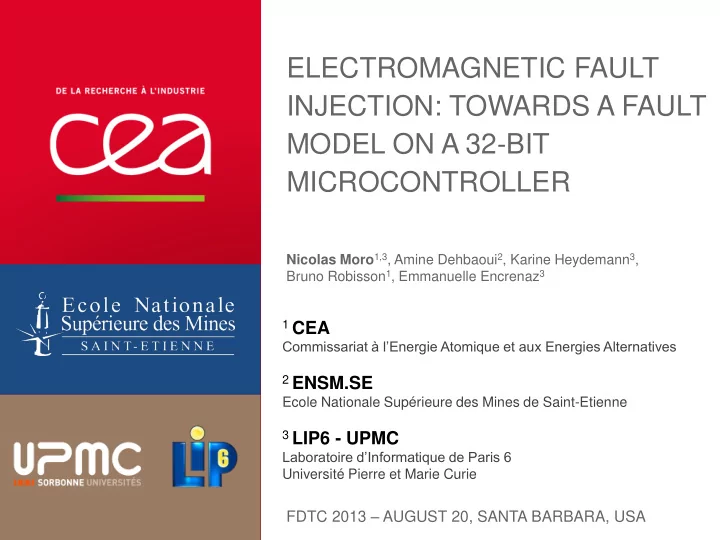
ELECTROMAGNETIC FAULT INJECTION: TOWARDS A FAULT MODEL ON A 32-BIT MICROCONTROLLER Nicolas Moro 1,3 , Amine Dehbaoui 2 , Karine Heydemann 3 , Bruno Robisson 1 , Emmanuelle Encrenaz 3 1 CEA Commissariat lEnergie Atomique et aux Energies
ELECTROMAGNETIC FAULT INJECTION: TOWARDS A FAULT MODEL ON A 32-BIT MICROCONTROLLER Nicolas Moro 1,3 , Amine Dehbaoui 2 , Karine Heydemann 3 , Bruno Robisson 1 , Emmanuelle Encrenaz 3 1 CEA Commissariat à l’Energie Atomique et aux Energies Alternatives 2 ENSM.SE Ecole Nationale Supérieure des Mines de Saint-Etienne 3 LIP6 - UPMC Laboratoire d’Informatique de Paris 6 Université Pierre et Marie Curie FDTC 2013 – AUGUST 20, SANTA BARBARA, USA | PAGE 1
MOTIVATIONS Security of microcontroller-based embedded systems against fault injection attacks Target : ARM Cortex-M3 microcontroller Fault injection means : Pulsed electromagnetic fault injection Theoretical attacks rely on an attacker’s fault model Electromagnetic fault injection is quite recent Very few in-depths studies of the effects on complex systems Better understanding of the effects of EM fault injection Detailed fault model at a register-transfer level FDTC 2013 – Santa Barbara, USA 9 OCTOBRE 2013 | PAGE 2
OUTLINE I. Experimental setup II. General approach III. Study of the injection parameters IV. Register-transfer level fault model V. Conclusion FDTC 2013 – Santa Barbara, USA | PAGE 3
FAULT INJECTION ATTACKS Perturbation C M K 010110000110011 Comparison 0110010101100001 110101000101101 Faulty ciphertext Several physical ways to inject faults into a circuit’s computation Necessary for an attacker to know the type of injected faults Fault target Data, instructions Fault type Bit flip, reset at 0, set at 1, stuck Granularity Bit, byte, word Determinism Deterministic, metastable, random Temporal aspect Single piece of data/instruction, multiple I – Experimental setup FDTC 2013 – Santa Barbara, USA OCTOBER 9, 2013 | PAGE 4
EXPERIMENTAL SETUP Pulsed electromagnetic fault injection Transient and local effect of the fault injection Standard circuits not protected against this technique Solenoid used as an injection antenna Up to 200V sent on the injection antenna, pulses width longer than 10ns Microcontroller based on an ARM Cortex-M3 - Frequency 56 MHz -16/32 bits Thumb2 RISC instruction set - ARMv7-M modified Harvard architecture - SWD link to debug the microcontroller I – Experimental setup FDTC 2013 – Santa Barbara, USA 9 OCTOBRE 2013 | PAGE 5
DETAILED EXPERIMENTAL PROTOCOL Experiment driven by the computer Execution of a computation on the target device Sending of a voltage pulse Stop of the microcontroller Harvesting of the microcontroller’s internal data Analysis of the obtained results Main experimental parameters • Position of the injection antenna • Electric parameters of the pulse • Injection time of the pulse • Executed code on the microcontroller I – Experimental setup FDTC 2013 – Santa Barbara, USA | PAGE 6
OUTLINE I. Experimental setup II. General approach III. Study of the injection parameters IV. Register-transfer level fault model V. Conclusion FDTC 2013 – Santa Barbara, USA | PAGE 7
GENERAL APPROACH Exhaustive instruction simulation (finds instructions which could enable to reach B’ from A) Experimental fault B’ (depends on the experimental parameters) Fault injection Initial state Expected state A B Instruction Output pieces of data Detail R0 to R12 General-purpose registers R13 (SP) Stack pointer R14 (LR) Link register R15 (PC) Program counter XPSR Program Status Register - Flags - Details about the triggered interruptions - Details about the execution mode Memory address that contains the calculation’s output Result II – General approach FDTC 2013 – Santa Barbara, USA 9 OCTOBRE 2013 | PAGE 8
SIMULATION OF A FAULT MODEL Instruction skip simulation Experimental measurements Two lines are equal R0 to R12 + XPSR + result + SP + PC are equal II – General approach FDTC 2013 – Santa Barbara, USA 9 OCTOBRE 2013 | PAGE 9
SIMULATION OF A FAULT MODEL Example of simulation of a 16-bit instruction replacement Very long for an exhaustive simulation over the whole instruction set Two lines are equal R0 to R12 + XPSR + result are equal II – General approach FDTC 2013 – Santa Barbara, USA 9 OCTOBRE 2013 | PAGE 10
OUTLINE I. Experimental setup II. General approach III. Study of the injection parameters IV. Register-transfer level fault model V. Conclusion FDTC 2013 – Santa Barbara, USA | PAGE 11
INFLUENCE OF THE ANTENNA’S POSITION Green : hardware interrupts have been triggered Red : faults on the output value have been obtained t = 0.4 ns t = 1 ns t = 2 ns t = 3.6 ns Frequency 56 MHz – Pulse width 10 ns – Pulse voltage 190V – Period 17ns t = 16.8 t = 18.6 t = 19.2 ns t = 20 ns ns ns Target instruction : single LOAD instruction that loads 0x12345678 into R8 20 ns time interval, by steps of 200 ps - 3 mm square, by steps of 200 µm Variable increase of the Hamming weight of the loaded piece of data No fault on other registers than R8 (except for very few faults on R0) III – Study of the injection parameters FDTC 2013 – Santa Barbara, USA | PAGE 12
INFLUENCE OF THE INJECTION TIME Example of temporal cartography on an addition loop 0xfb 0xf7 0xef 0xdf 0xbf 0x7f 0xfe 0xfd Test program: Observations: loop to sum the elements of an array One power of two has not been added that contains eight powers of two 3.5 µs, by steps of 200 ps BusFault or UsageFault interrupts Expected result: 0xFF Does our fault injection have an effect on the data flow or the control flow ? III – Study of the injection parameters | PAGE 13 FDTC 2013 – Santa Barbara, USA
INFLUENCE OF THE PULSE’S VOLTAGE LDR R4, PC#44 with 0x12345678 at the address PC#44 Pulse voltage Output value Occurrence rate 172V 1234 5678 100 % 174V 9 234 5678 73 % 176V FE 34 5678 30 % 178V FFF 4 5678 53 % 180V FFFD 5678 50 % 182V FFFF 7F 78 46 % 184V FFFF FFFB 40 % 186V FFFF FFFF 100 % Simulation : corresponds to no instruction replacement Looks like a set at 1 fault model on the Flash memory data transfers Possible precharge of the data bus on this architecture III – Study of the injection parameters FDTC 2013 – Santa Barbara, USA 9 OCTOBRE 2013 | PAGE 14
OUTLINE I. Experimental setup II. General approach III. Study of the injection parameters IV. Register-transfer level fault model V. Conclusion FDTC 2013 – Santa Barbara, USA | PAGE 15
FAULTS ON THE CONTROL FLOW Experiments with a sequence of NOP (BF 00) Four kinds of faults Fault on R7 The program does not stop UsageFault exceptions (Invalid Instruction / No Coprocessor) Fault on R0 Sometimes a modification of the number of executed cycles Simulation on the ISA: some instructions can explain the results Some faults only equivalent to a STR R0, [R0, #0] instruction NOP - BF00 1011 1111 0000 0000 STR R0, [R0, #0] - 6000 0110 0000 0000 0000 NOP - BF00 1011 1111 0000 0000 NOP - BF00 1011 1111 0000 0000 IV – Register-transfer level fault model FDTC 2013 – Santa Barbara, USA | PAGE 16
INSTRUCTION FETCH Normal behaviour IV – Register-transfer level fault model FDTC 2013 – Santa Barbara, USA 9 OCTOBRE 2013 | PAGE 18
INSTRUCTION FETCH With an electromagnetic fault injection IV – Register-transfer level fault model FDTC 2013 – Santa Barbara, USA 9 OCTOBRE 2013 | PAGE 19
DATA LOAD FROM THE FLASH MEMORY Normal behaviour IV – Register-transfer level fault model FDTC 2013 – Santa Barbara, USA 9 OCTOBRE 2013 | PAGE 20
DATA LOAD FROM THE FLASH MEMORY With an electromagnetic fault injection IV – Register-transfer level fault model FDTC 2013 – Santa Barbara, USA 9 OCTOBRE 2013 | PAGE 21
OVERVIEW OF THE DEFINED FAULT MODEL Possible to fault the transfers from the Flash memory Consequences regarding the instruction flow Instructions replacements Instruction skips under certain conditions (~ 20-30% of time) Some instructions may be more sensitive than others Some registers seem to be more sensitive than others Consequences regarding the data flow Corruption of the LOAD instructions from the Flash memory (encryption keys ,…) Some metastability phenomena, but deterministic under some conditions Faulty values with higher Hamming weight (on this architecture) IV – Register-transfer level fault model FDTC 2013 – Santa Barbara, USA 9 OCTOBRE 2013 | PAGE 22
OUTLINE I. Experimental setup II. General approach III. Study of the injection parameters IV. Register-transfer level fault model V. Conclusion FDTC 2013 – Santa Barbara, USA | PAGE 23
CONCLUSION AND PERSPECTIVES A first attempt of fault model for EM fault injection on a 32-bit µC Corruption of the transfers from the Flash memory on the buses The obtained effects seem very similar to the ones obtained with clock glitches or other fault injection means Similar effects obtained previously on a very different architecture (Atmel AVR ATmega128 8-bit microcontroller) Possibility to perform instruction skips under some specific conditions Perspectives • Use more advanced debug techniques to understand better instruction replacements • Define a higher-level fault model that can be used for theoretical attacks FDTC 2013 – Santa Barbara, USA Conclusion 9 OCTOBRE 2013 | PAGE 24
THANK YOU FOR YOUR ATTENTION Any questions ? FDTC 2013 – Santa Barbara, USA Conclusion 9 OCTOBRE 2013 | PAGE 25
Recommend
More recommend
Explore More Topics
Stay informed with curated content and fresh updates.

