Memory Hierarchy Instructor: Jun Yang 1 11/19/2009 Motivation - PowerPoint PPT Presentation
Memory Hierarchy Instructor: Jun Yang 1 11/19/2009 Motivation Processor-DRAM Memory Gap (latency) Proc 1000 CPU 60%/yr. Moores Law (2X/1.5yr) Performance 100 Processor-Memory Performance Gap: (grows 50% / year) 10 DRAM
Memory Hierarchy Instructor: Jun Yang 1 11/19/2009
Motivation Processor-DRAM Memory Gap (latency) µProc 1000 CPU 60%/yr. “Moore’s Law” (2X/1.5yr) Performance 100 Processor-Memory Performance Gap: (grows 50% / year) 10 DRAM 9%/yr. DRAM (2X/10 yrs) 1 1980 1981 1982 1983 1984 1985 1986 1987 1988 1989 1990 1991 1992 1993 1994 1995 1996 1997 1998 1999 2000 Time 11/19/2009 2
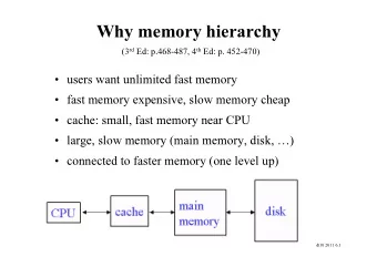
The Goal: Illusion of Large, Fast, Cheap Memory • Goal: a large and fast memory • Fact: Large memories are slow Fast memories are small • How do we create a memory that is large, cheap and fast (most of the time)? – Hierarchy 11/19/2009 3
Memory Hierarchy of a Modern Computer System • By taking advantage of the principle of locality: – Present the user with as much memory as is available in the cheapest technology. – Provide access at the speed offered by the fastest technology. Processor Control Tertiary Secondary Storage Storage (Tape) Off-Chip Main (Disk) Caches Memory Registers On-Chip Caches Datapath (SRAM) (DRAM) 10,000,000,000s 10,000,000s Speed (ns): 1s 10s 100s (10s sec) (10s ms) Size (bytes): 100s Ks Ms Gs Ts 11/19/2009 4
Memory Hierarchy: Why Does it Work? Locality! Probability of reference 0 2^n - 1 Address Space • Temporal Locality (Locality in Time): => Keep most recently accessed data items closer to the processor • Spatial Locality (Locality in Space): => Move blocks consists of contiguous words to the upper levels Lower Level Upper Level Memory To Processor Memory Blk X From Processor Blk Y 11/19/2009 5
Memory Hierarchy Technology • Rando dom m Access: – “Random” is good: access time is the same for all locations – DRAM: Dynamic Random Access Memory • High density, low power, cheap, slow • Dynamic: need to be “refreshed” regularly – SRAM: Static Random Access Memory • Low density, high power, expensive, fast • Static: content will last “forever”(until lose power) • “Not ot-so so-random” Acces ess Tec Technology: – Access time varies from location to location and from time to time – Examples: Disk, CDROM • Seq Sequential Acces ess Tec Technology: access time linear in location (e.g.,Tape) • We will concentrate on random access technology – The Main Memory: DRAMs + Caches: SRAMs 11/19/2009 6
Introduction to Caches • Cache – is a small very fast memory (SRAM, expensive) – contains copies of the most recently accessed memory locations (data and instructions): temporal locality – is fully managed by hardware (unlike virtual memory) – storage is organized in blocks of contiguous memory locations: spatial locality – unit of transfer to/from main memory (or L2) is the cache block • General structure – n blocks per cache organized in s sets – b bytes per block – total cache size n*b bytes 11/19/2009 7
Caches • For each block: – an address tag : unique identifier – state bits: • (in)valid • modified – the data: b bytes • Basic cache operation – every memory access is first presented to the cache – hit: the word being accessed is in the cache, it is returned to the cpu – miss: the word is not in the cache, • a whole block is fetched from memory (L2) • an “old” block is evicted from the cache (kicked out), which one? • the new block is stored in the cache • the requested word is sent to the cpu 11/19/2009 8
Direct Mapped Cache • Cache stores a subset of memory blocks • Mapping: address is modulo the number of blocks in the cache Cache 000 001 010 011 111 100 101 110 00001 00101 01001 01101 10001 10101 11001 11101 9 Memory
Block Size > 4 bytes (1 word) 00 01 10 11 01010 11110 01011 11111 00000 00001 00010 00100 00101 10000 10001 10100 10101 00011 10
Two way set-associative mapping 4 bytes per block Way 1 Way 0 00 01 10 00 01 10 11 11 00000 00001 00010 00011 11
Addressing the Cache – Direct mapped cache: one block per set. log n log b Direct mapping tag index offset – Set-associative mapping: n/s blocks per set. log b log n/s Set-associative mapping tag index offset – Fully associative mapping: one set per cache (s = n). Fully associative mapping log b tag offset 12
Example: 1 KB Direct Mapped Cache with 32 B Blocks • For a 2 N byte cache: – The uppermost (32 - N) bits are always the Cache Tag – The lowest M bits are the Byte Select (Block Size = 2 M ) – One cache miss, pull in complete “Cache Block” (or “Cache Line”) Block address 31 9 4 0 Cache Tag Example: 0x50 Cache Index Byte Select Ex: 0x01 Ex: 0x00 Stored as part of the cache “state” Valid Bit Cache Tag Cache Data Byte 31 Byte 1 Byte 0 0 : 0x50 Byte 63 Byte 33 Byte 32 1 : 2 3 : : : Byte 1023 Byte 992 31 : 13
Set Associative Cache Architecture • N-way set associative: N entries for each Cache Index – N direct mapped caches operates in parallel • Example: Two-way set associative cache – Cache Index selects a “set” from the cache – The two tags in the set are compared to the input in parallel – Data is selected based on the tag result Cache Index Valid Cache Tag Cache Data Cache Data Cache Tag Valid Cache Block 0 Cache Block 0 : : : : : : Adr Tag Compare Compare 1 0 Mux Sel1 Sel0 OR Cache Block Hit 14
Example: Fully Associative Architecture • Fully Associative Cache – Forget about the Cache Index – Compare the Cache Tags of all cache entries in parallel – Example: Block Size = 32 B blocks, we need N 27-bit comparators • By definition: Conflict Miss = 0 for a fully associative cache 31 4 0 Cache Tag (27 bits long) Byte Select Ex: 0x01 Cache Tag Valid Bit Cache Data = Byte 31 Byte 1 Byte 0 : = Byte 63 Byte 33 Byte 32 : = = : : : = 15
Cache Organization – Example • Instruction & Data caches: –Because instructions have much lower miss rates: split the cache (at L1 level) into instruction and data. Otherwise, unified. –Main advantages: no interference, data misses do not stall instruction fetch, optimize for different access patterns etc. • AMD Opteron Cache –64K I & D caches (L1), 2-way set associative; –b = 64 bytes; –write-back; write allocate on write miss. –Organization shown in Fig. 5.19 –Read & write hits: 2 cycles, pipelined. –Victim buffer: 8 entries. 16
Alpha 21264 Cache Organization 17
Block Replacement • Block replacement – not an issue with direct mapped – replacement strategy is more important in small caches than in large ones – replacement policies: • LRU: has been unused for the longest time. good temporal locality, complex state • pseudo-random: randomly selected • FIFO: oldest block. Difference with LRU? 18
LRU example • Assume a fully-associative cache with two blocks, which of the following memory references miss in the cache. 0 Tags 1 LRU addresses – assume distinct -- -- 0 A addresses go to distinct blocks B A C B A B 19
LRU example • Assume a fully-associative cache with two blocks, which of the following memory references miss in the cache. 0 Tags 1 LRU addresses -- -- 0 miss A On a miss, we A -- 1 replace the LRU. miss B A B 0 A On a hit, we j ust A B 1 update the LRU. miss C A C 0 miss B B C 1 miss A B A 0 B B A 1 20
Exercise • Assume you have a fully associative cache with 4 entries. For the following memory block address sequence, which entry becomes the LRU at the end? 8 9 5 2 6 5 9 10 3 21
Write Policies • Writes are hard • Trade-offs – read: concurrently check tag – Write-back: and read data • uses less bus bandwidth, – write is destructive, so it must be slower – Write-through: • keeps MM consistent with • Write strategies CM, – when to update memory? • good for DMA. • on every write ( write-through ) • when a modified block is replaced ( write-back ) – what to do on a write miss? • fetch the block to cache ( write allocate ), used with write-back • do not fetch ( write around ), used with write-through 23
Write Buffers • Write-through Buffers • Write-back Buffers – between a write-back cache and – buffers words to be written in L2 or MM L2 cache/memory along with – algorithm their addresses. • move dirty block to write-back – 2 to 4 entries deep buffer – all read misses are checked • read new block against pending writes for • write dirty block in L2 or MM dependencies (associatively) – can be associated with victim cache (later) – can coalesce writes to same address to CPU L1 Write buffer L2 24
Improving CPU Performance • In the past 10 years, there are over 5000 research papers on reducing the gap between the CPU and memory speeds. • We will address some them in four categories: – Reducing the miss rate – Reducing the cache miss penalty – Reducing the cache miss penalty or miss rate via parallelism – Reducing the hit time 29
Recommend
More recommend
Explore More Topics
Stay informed with curated content and fresh updates.

