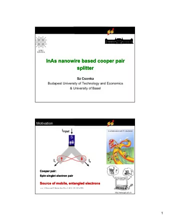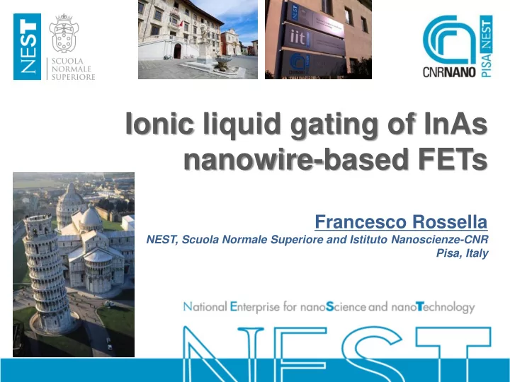
Ionic liquid gating of InAs nanowire-based FETs Francesco Rossella - PowerPoint PPT Presentation
Ionic liquid gating of InAs nanowire-based FETs Francesco Rossella NEST, Scuola Normale Superiore and Istituto Nanoscienze-CNR Pisa, Italy NEST, Scuola Normale Superiore & Istituto Nanoscienze-CNR A public institute for higher education
Ionic liquid gating of InAs nanowire-based FETs Francesco Rossella NEST, Scuola Normale Superiore and Istituto Nanoscienze-CNR Pisa, Italy
NEST, Scuola Normale Superiore & Istituto Nanoscienze-CNR A public institute for higher education and research Palazzo Carovana, SNS http://www.laboratorionest.it/
Nanowire-based devices Materials: self-assembled NW heterostructures
Nanowire-based devices Materials: self-assembled NW heterostructures Technology: field effect controlled NW-based devices
Nanowire-based devices Materials: self-assembled NW heterostructures Technology: field effect controlled NW-based devices Experiments: electrical & thermal transport, luminescence
Nanowire-based devices Materials: self-assembled NW heterostructures Technology: field effect controlled NW-based devices Experiments: electrical & thermal transport, luminescence Targets: fucntional devices: (Q)ICTs, energy harvesting
Nanowire-based devices Materials: self-assembled NW heterostructures Technology: field effect controlled NW-based devices Experiments: electrical & thermal transport, luminescence Targets: fucntional devices: (Q)ICTs, energy harvesting Implementation: I. hemogeneous nanowires II. InAs/InP axial heterostructures III. InAs/InP/GaSb radial heterostructures IV. Hybrid metal/semiconductor axial heterostrictures
Nanowire-based devices Materials: self-assembled NW heterostructures Technology: field effect controlled NW-based devices Experiments: electrical & thermal transport, luminescence Targets: fucntional devices: (Q)ICTs, energy harvesting Implementation: I. homogeneous nanowires II. InAs/InP axial heterostructures III. InAs/InP/GaSb radial heterostructures IV. Hybrid metal/semiconductor axial heterostrictures
Nanowire growth by CBE gaseous NW Lucia reactant nucleation Sorba Chemical beam catalyst epitaxy III-V Semiconductors Self-assembled Au catalyst nanocrystals Chemical Beam Epitaxy (bottom-up approach)
Nanowire growth by CBE Daniele Valentina Ercolani Zannier Au colloids Au film EBL-defined dots Isha Omer Verma Arif
Nanowire growth by CBE Au thin film Daniele Valentina Ercolani Zannier Au colloids Au film EBL-defined dots Gomes et al ., SST 30 , 115012 (2015) Isha Omer Verma Arif
Nanowire growth by CBE Au thin film Daniele Valentina Ercolani Zannier Au colloids Au film EBL-defined dots Gomes et al ., SST 30 , 115012 (2015) EBL-defined dots 30 NW Counts 20 10 0 0 10 20 30 40 50 60 70 80 Isha Omer Verma Arif
Radial heterostructures: core-shell NWs Zhara InAs core Umesh Montmatz Gomes 200 nm 100 nm Mirko ~0.8eV GaSb shell Rocci GaSb e Tunable Esaki effect h Thermoelectrics in coupled 1D systems ~0.4eV InAs 1D-1D Coulomb drag S.Pezzini , … and F.Rossella, i n preparation M.Rocci, F.Rossella* et al., Nano Lett. 16 , 7950 (2016)
Axial heterostructures GaAs/InAs Sharp interface between 2 semiconductors
Axial heterostructures GaAs/InAs InAs/InP S. Roddaro Sharp interface InP barriers few nm thick between 2 semiconductors inside an InAs NW Tunneling processes in 0D and 1D (NW-QDs) Shottcky barriers light emission, optoelectronics
Axial heterostructures GaAs/InAs InAs/InP Hybrids S. Roddaro M. 100 nm Gemmi J. David V. Piazza Sharp interface InP barriers few nm thick Metal/semiconductor between 2 semiconductors inside an InAs NW junctions Tunneling processes in 0D and 1D (NW-QDs) Shottcky barriers light emission, optoelectronics J. David, F. Rossella* et al, Nano Lett. 17 , 2336 (2017) F. Rossella* et al, Nano Lett . 16 , 5521 (2016) F. Rossella et al, Nat. Nanotech. 9 , 997 (2014); F. Rossella et al, J. Phys. D: Appl. Phys . 47 394015 (2014) L. Romeo et al., Nano Lett. 12, 4490 (2012); S. Roddaro et al., Nano Lett. 11 , 1695 (2011)
Homostructures: graded n-type doping A. Tredicucci A. Arcangeli s-SNOM n(x) ε (x) tailoring dielectric response Semiconductor gate-tunable nano-plasmonics A.Arcangeli, F. Rossella* et al, Nano Lett. 16 , 5688 (2016)
Ionic liquid gating of InAs nanowire-based FETs V. Demontis, V. Zannier, D. Ercolani, L. Sorba, F. Beltram and F. Rossella S. Ono J. Lieb and B. Sacepe NEST, Scuola Normale Superiore and Istituto Nanoscienze-CNR, Pisa (Italy) Central Research Institute of Electric Power Industry, Yokosuka, Kanagawa (Japan) Univ. Grenoble Alpes, CNRS, Grenoble INP, Institut Neel, Grenoble (France)
NW Thermoelectrics SUPPORTED NW devices: Seebeck & Power Factor 2 S ZT T l k k e
NW Thermoelectrics SUPPORTED NW devices: Seebeck & Power Factor 2 S ZT T l k k e V 0 -V H V 0 +V H Differential bias 2 V H S.Roddaro, et al., Nano Research 2014
NW Thermoelectrics SUPPORTED NW devices: Seebeck & Power Factor 2 S ZT T l k k e V 0 -V H V 0 +V H Differential bias 2 V H S.Roddaro, et al., Nano Lett. 2013 S.Roddaro, et al., Nano Research 2014
NW Thermoelectrics SUPPORTED NW devices: Seebeck & Power Factor 2 S ZT T D.Prete et al, in preparation 2018 l k k E. Tickonov, et al. Sci. Rep. 2016 e E. Tickonov, et al. SST 2016 V 0 -V H V 0 +V H Differential bias 2 V H S.Roddaro, et al., Nano Lett. 2013 S.Roddaro, et al., Nano Research 2014
NW Thermoelectrics SUSPENDED NW devices: thermal conductivity 2 S ZT T l k k e
NW Thermoelectrics SUSPENDED NW devices: thermal conductivity 2 S ZT T l k k e Optical approach S. Yazi, et al., Nano Research 2015
NW Thermoelectrics SUSPENDED NW devices: thermal conductivity 2 S ZT T l k k e Optical approach All-electrical method: Current injection at freq ω Voltage probing at freq 3 ω S. Yazi, et al., Nano Research 2015 M.Rocci et al, submitted 2018
Suspended NW devices: strategies for gating? backgate, side gates poor modulation of σ at temperatures of interest F.Rossella et al, Semiconductor and Semimetals 2018 15% R modulation within +/- 20V (combining BG and SG)
Ionic liquid gating
Zoology of ionic liquids CATIONS ANIONS
Zoology of ionic liquids Made for each other! CATIONS ANIONS
BMI+ PF6- DFT InAs InAs Hexafluorophosphate (coarse grain) -q q + layered electrodes + porosity Molecular dynamics diffusion coefficients V. Tozzini L. Bellucci
Many additional problems in simulations! realistic structure of the porosity (→ sponge builder) Size of the system The model of electrode must be polarizable Tests to validate the Test with mechanically induced diffusion: model anion has a larger diffusivity than the cation optimize the simulation parameters Test with nanoporous charged polarizable electrodes
Electric Double Layer Transistors & Thermoelectrics • Test-bed for confinement effects (DOS discretization) ZT, S 2 σ enhancement • oxides (SrTiO3, ZnO, Cu2O) Thin films 2D materials SWCNTs NWs ??
Ionic liquid gated InAs NW FET: realization
Ionic liquid gated InAs NW FET: realization
Ionic liquid gated InAs NW FET: realization
Ionic liquid gated InAs NW FET: realization
Ionic liquid gated InAs NW FET: realization J. Lieb , … and F.Rossella, submitted
Hysteresis (getting rid of) Parameter space: • Temperature
Hysteresis (getting rid of) Parameter space: • Temperature • d V LG /dt (liquid gate voltage Sweep rate)
Hysteresis (getting rid of) Parameter space: • Temperature • d V LG /dt (liquid gate voltage Sweep rate) T = 240 K d V LG /dt < 10 mV/s
Hysteresis (getting rid of) 2.4 2.3 W I DS ( A) 2.2 MIN I DS 2.1 MIN V LG 2.0 -2 -1 0 1 2 V LG (V)
Hysteresis (getting rid of) T (K) 220 240 260 280 300 2.4 4mV/s 2 W (V) 1 2.3 0 W -0.5 I DS ( A) LG (V) 2.2 -1.0 MIN V -1.5 MIN I DS 2.2 2.1 DS ( A) 2.0 MIN V MIN LG 1.8 2.0 I 220 240 260 280 300 -2 -1 0 1 2 V LG (V) T (K)
Hysteresis (getting rid of) sweep rate (mV/s) T (K) 220 240 260 280 300 0 40 80 120 2.4 4mV/s 2 2 W (V) W (V) 1 1 2.3 0 0 W -0.5 -0.5 I DS ( A) LG (V) LG (V) 2.2 -1.0 -1.0 MIN MIN V V -1.5 -1.5 MIN I DS 2.2 2.2 2.1 DS ( A) DS ( A) 2.0 2.0 MIN V MIN MIN LG 1.8 1.8 2.0 I I 220 240 260 280 300 0 40 80 120 -2 -1 0 1 2 sweep rate (mV/s) V LG (V) T (K)
Ionic liquid gated InAs NW FET: operation < 100 pA Full pinch-off
Ionic liquid gated InAs NW FET: operation < 100 pA Full pinch-off Linear & saturation regions
Ionic Liquid Gate vs back gate LIQUID GATE
Ionic Liquid Gate vs back gate LIQUID GATE BACK GATE (no liquid) n ≈ 5*10 17 cm -3 µ ≈ 200 cm 2 /Vs C BG ≈ 60 aF
Ionic Liquid Gate vs back gate LIQUID GATE BACK GATE (no liquid) BOTH (same device) n ≈ 5*10 17 cm -3 µ ≈ 200 cm 2 /Vs C BG ≈ 60 aF C LIQUID GATE ≈ 30* C BG
Gate induced transition
Gate induced transition V LG << 0V semiconductor V LG >> 0 V Metal-like
Recommend
More recommend
Explore More Topics
Stay informed with curated content and fresh updates.
