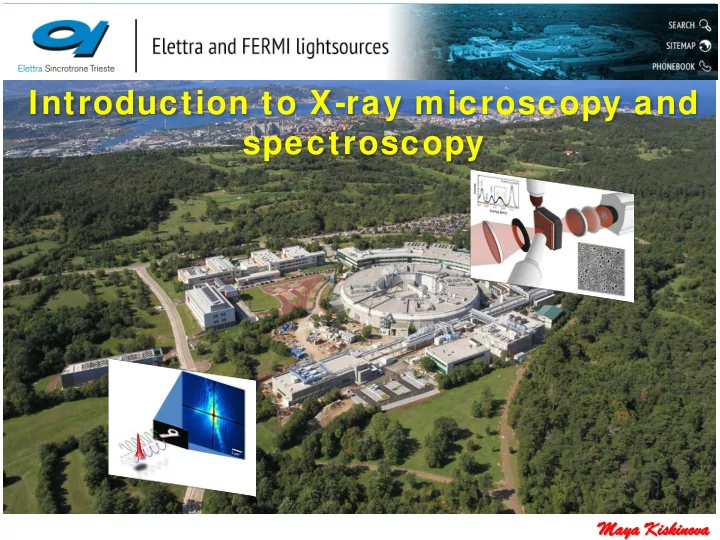
Introduction to X-ray microscopy and spectroscopy Maya a Kisk - PowerPoint PPT Presentation
Introduction to X-ray microscopy and spectroscopy Maya a Kisk skinova An Invitation to Enter a New Field of Physics & Material Science Richard P. Feynman - 1959!!! There's Plenty of Room at the Bottom NANO N NO by nature,
Introduction to X-ray microscopy and spectroscopy Maya a Kisk skinova
An Invitation to Enter a New Field of Physics & Material Science Richard P. Feynman - 1959!!! There's Plenty of Room at the Bottom ‘NANO’ ‘N NO’ by nature, design o by or externally lly- indu duced c cha hanges • Materials have properties varying at various depth and length scales and are usually laterally inhomogeneous at atomic, nano or meso scales. • Structure and chemical composition usually is different at the surface and in the bulk. • New properties expected with decreasing the dimensions stepping into nanoworld. What we NEED: Chemical sensitivity, spatial resolution & morphology & structure, varying probing depth, temporal resolution when possible. Majority of these methods are based on interaction of the matter with photon, electron or ion radiation. Maya a Kisk skinova
Why Microscopy needs Synchrotrons tunable High Brightness % coherent polarized Synchrotron light advantages Very bright, wave-length tunable (cross sections and atomic edges), multiply polarized (dichroic effects, bonding orientation), partly coherent. Great variety of spectroscopies - elemental, chemical, magnetic information Variety of imaging contrasts based on photon absorption, scattering or spectroscopic feature. Higher penetration power compared to charged particles - less sensible to sample environment . Maya a Kisk skinova
All methods using SR are based on the interaction of photons with the matter and find applications in all domains of science and technology λ λ θ nul d λ X-ray Absorption Spectroscopy (XAS) and InfraRed Absorption Spectroscopy θ (IRAS) λ θ d X-ray Photoelectron Spectroscopy (XPS) Auger Electron Spectroscopy (AES) and XAS Fluorescence Spectroscopy (FS) and XAS Maya a Kisk skinova
Spectroscopies @ synchrotron light sources: XPS-AES, XRF, XAS, RIXS Photoelectric effect & de-excitation processes = chemical specific spectroscopies FS FS XPS FS AES E h ν = constant & energy filtering of emitted photons and electrons h ν out h ν in/e - out e - out PES+AES PES=XPS+AES XAS: based on absorption coefficient µ = f(h ν -E core ) and resonant electronic transitions governed by selection rules e - and h ν detection E h ν scanned Maya a Kisk skinova
Sampling depths: depend on the detected signal (electrons or photons) Fluorescence emission (XAS and FS): TEY& Auger electron emission (XAS), core&valence PES: Probe depth 1- 10 nm Probe depth > 100 nm = f(E ph , matrix) FS X-ray transmission: ‘bulk’ Maya a Kisk skinova
Microscopic Approaches, Adding Spatial Resolution: X-ray or electron optics SPEM Lateral resolution using Lateral resolution provided by photon optics electron optics Maya a Kisk skinova
X-ray focusing optics: zone plates, mirrors, capillaries KP-B mirrors each focusing in one direction: soft & hard X- rays: ~ 100 nm Soft & hard x-rays! Zone Plate optics – circular XFS,XPS, achromatic focal point, easy grating with decreasing width: XANES energy tunability, comfortable from ~ 200 to ~ 10000 eV working distance Monochromatic: Resolution ≤ 100 nm Resolution achieved 15 nm in transmission Capillary: multiple reflection Refractive lenses concentrator Normal incidence: spherical mirrors with multilayer interference coating (Schwarzschild Objective) Hard x-rays ~ 4-70 keV Monochromatic, good for E < 100eV Resolution: > 1000 nm Hard x-rays ~ 8-18 keV Resolution: best ~ 100 nm Resolution: > 3000 nm Maya a Kisk skinova
Zone plate : circular diffraction grating of N lines with radially decreasing line width operating in transmission dr N OSA m=0 1 2 t 3 f -1 f 1 f -2 f -3 f 3 f 2 D f m = D.dr N / λ Important parameters: Finest zone width, dr N (10-100 nm) - determines the Rayleigh resolution (microprobe size) δ t =0.61 λ /( θ ) =1.22 δ r N Diameter, D (50-250 µ m), dr N and λ determine the focal distance f. Efficiency % of diffracted x-rays: 10-40% (4-25%) Monochromaticity required: λ /d λ ≥ N (increases with dr and D ). Maya a Kisk skinova
X-ray transmission microscope (TXM-FFIM) Full-field X-ray imaging or “one shot” X-ray image acquisition can be considered CCD camera as the optical analog to visible light transmission microscope. Günther Schmahl, 1st experiment DESY 1976 Objective ZP to magnify the image Aperture: onto the detector removes (i) unwanted diffraction orders and straylight, and serves (ii) with condenser as monochromator Specimen environment: to be X-ray light adapted to application from a 2 nd or 3 rd generation light Condenser source illuminating the object field Resolution achieved better than 15 nm. Maya a Kisk skinova
Following dynamic processes during temperature treatment, applying magnetic/electric field or pumping with optical lasers X Fe38Rh62 nanoparticles XAS-XMCD X-Ray Magnetic Circular Dichroism Maya a Kisk skinova
Cryogenic 3D imaging of biological cells Maya a Kisk skinova
X-ray Scanning microscopy: uses focusing x-ray optics (preferred zone plates) Works in Transmission and Emission + microspot spectroscopy Janos Kirz, 1st operating STXM 1983 SPEM 1990 e - or x-ray detector incl. spectroscopy Can use all detection modes! Resolution achieved 25 nm in transmission. Maya a Kisk skinova
Microscopy Approaches @ ELETTRA storage ring : X-ray or electron optics; X-ray or electron detection Magnetic imaging PES Imaging and microspectroscopy XRF, XPS, XAS = elemental and chemical information X-ray transmission and scattering (phase contrast) - morphology Topology – electron emission XRF Fe 2 XPEEMs – Elettra & FZJ + Spin filtered detection 3 Scanning x-ray microscopes Co ABS 3 1 4 2 5 The image contrast can provide: Microspectroscopy: Morphology: density, thickness (transmission) μ - XPS, μ - XANES, μ -XRF in selected areas Element presence and concentration- e - , h ν ; from the images: detailed characterization Chemical state, band-bending, charging e - ; of the chemical and electronic structure of Magnetic spin or bond orientation – e - , h ν coexisting micro-phases. Maya a Kisk skinova
Layout of SPEM: Focusing optics (ZP, SO or K-B), sample and positioning systems OSA ZP Spatial resolution in electron ZP emission limited by the sample-to-optics distance ! f m =D x dr x E ph / 1240 ~10 mm for soft X rays δ sample r = DOF f OSA m D Typical: 5-15 µ m Maya a Kisk skinova
SPEMs energy-filtering electron analyzers MCD developed @ ELETTRA Scanned sample MCP Micro Channel Plate N anodes E1 E16 e - Selected channels: MCP1 chemical state MCP2 48 channel anode detector E 0 + ∆ E E 0 E 0 - ∆ E V out Spectro-imaging µ -spectroscopy E 0 position sensitive concentration map V in detector Maya a Kisk skinova
Model catalyst systems studied with SPEM: single crystals and supported metal particles on MgO Oxidation states: Ru(Rh) 3d maps & Ru(Rh)3d µ-PES SEM SEM SPEM R. Blume et al, JPC B 109, 14058; P. Dudin et al, JPC B 109, 13649; 125, 94701 Ru(0001) Ξ Rh(110) Rh SPEM map advanced No simple size effect 2 µm Ru3d metallic state initial 32 µ m ‘Transient Surface Oxide’ (TSO) ~ 10-12 Å; Ru(Rh) oxides nucleate inside the ‘amorphous’ TSO P. Dudin et al, JPC C 1112, 9040; M. Dalmiglio JCP C, 114 16885 Maya a Kisk skinova
Correlation of the µm-particle reactivity to its complex surface structure: SPEM - LEEM LEEM µ-LEED O 2 • ‘Inhomogeneous’ reactivity in µ -Ps related to the surface morphology; • Structural evolution upon oxidation ends with a disordered oxide M. Dalmiglio, JPC-C 114, 2010, 16885. Maya a Kisk skinova
Degradation of organic light emission devices: mechanism revealed by ‘in-situ’ SPEM OLED exposed to ambient: moisture? supposed to be the damaging factor SPEM SPEM 1 µ -XPS 10 µ m Topographic features due to fracture: clearly seen as enhancement and shadowing of the emitted electrons Chemical imaging & µ-XPS revealed anode material (In and Sn) deposited around the hole created in the Al cathode of OLEDs. Maya a Kisk skinova
‘In-situ’ imaging of the local deformation and fracturing of the OLED cathode surface “Clean” failure experiment: OLED growth and operated in the SPEM (UHV ambient) Al maps In maps µ -XPS increasing voltage and operating time AFM and In maps of InSn oxide Al 2p map In 3d map C Evidence of InSn oxide and organic layer local decomposition, caused by spikes Lateral variations of the surface topography and chemistry of the InSn oxide anode films suggested as the major reasons for the device failures. P. Melpigniano et al, APL 86, 41105, S. Gardonio, Org.Electr. 9, 253 Maya a Kisk skinova
Exploring the properties of individual and free- standing nano-structures Low density NWs NB electronic nose Maya a Kisk skinova
SPEM characterization of MoS 2 -nanotubes Twisted chiral bundles of Mo-S individual cylinders: Mo 3d maps ? It that due to the low dimensionality the S 2p, Mo 3d and VB spectra are position- dependent? This should indicate electronic properties significantly different those of the MoS 2 crystal. SPEM revealed I (used as a carrier) in interstitial positions between the tubes bonded to the outer S atoms. ? Is the role of I ?? Maya a Kisk skinova
Recommend
More recommend
Explore More Topics
Stay informed with curated content and fresh updates.
