Interesting Properties of Strained or Defective Graphene ACS NANO - PowerPoint PPT Presentation
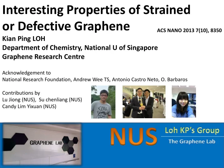
Interesting Properties of Strained or Defective Graphene ACS NANO 2013 7(10), 8350 Kian Ping LOH Department of Chemistry, National U of Singapore Graphene Research Centre Acknowledgement to National Research Foundation, Andrew Wee TS, Antonio
Interesting Properties of Strained or Defective Graphene ACS NANO 2013 7(10), 8350 Kian Ping LOH Department of Chemistry, National U of Singapore Graphene Research Centre Acknowledgement to National Research Foundation, Andrew Wee TS, Antonio Castro Neto, O. Barbaros Contributions by Lu Jiong (NUS), Su chenliang (NUS) Candy Lim Yixuan (NUS)
Graphene (dry) Graphene-oxide (wet) Grown by dry CVD process Planar structure Wet chemistry, from graphite High π electron density Non-stoichiometric COx bonding interactions Complex interplay of ionic and Governed by - interactions non-ionic intercations Pioneers: Rodney Ruoff, (U Texas) Byung Hee Hung (SKKU) Science 324 , 2009 , 1312 Nature Nanotechnology 5 , 2010 , 574 A giant polyaromatic framework that can mediate multiple interactions
A consequence of graphene being a soft membrane is that it can be strain- engineered to become highly corrugated by modifying its adhesion to the substrate.
As a soft membrane – Graphene is easily rippled I. Nanoripples Zhao wang et. al. Step edges (terrace) Typical Cu surface density~ 2.5 per um after growth Electron-flexural phonon scattering in such partially suspended graphene devices introduces anisotropic charge transport and limits charge mobility. Influence of Flexural phonon is reduced under tension. Applying weak strain may be enough CVDG/SiO2 with high density nanoripples Nanoripple density ~ 1.5 per um Guangxin Ni, O. Barbaros, ACS NANO, 6(2012) 1158
1. Periodically Strained Graphene as a Reaction Breadboard
Graphene Moire Superstructure on Ruthenium: A Strained Reaction Breadboard 1300 K for 3-5 mins RT Θ > 1ML C 60 T > 1000 o C Annealing 3 mins Single crystal graphene buckling instability due to the compressive strain between lattice- mismatched Ru and G produces moire pattern 2 nm 40 nm One inspiration from looking at the periodic blisters on the Moiré superlattice is the remarkable resemblance of these blisters to an ordered array of nano-bubbles !!
Moire Superlattice as Reaction Breadboad: Example 1: Selective Hydrogenation Occurs on the Hump Region of the Moire Superlattice Yu Wang and K. P. Loh, ACS NANO, 4, 6146 (2010) Hump region is a sink for diffusing H atoms d. H adsorption at room temperature, random cluster e. After annealing to 300 deg C, ordered cluster on bright regions of moire = hump. f,g: after annealing to cause H desorption
Reaction Breadboard Example 2: Contrasting Potential Energy Landscape on the Moire Surface Rotation of C60 frozen on Moire Valley BUT free Rotation of C60 on Moire Hump Jiong Lu, K. P. Loh, ACS Nano , 2012, 6 (1), pp 944 – 950 C60 in the hump B C60 in the valley A C60 in the rim In one unit cell, Rim: hump: valley = 6:1:1
Using the Graphene Moiré Pattern for the Trapping of C60 and Homoepitaxy of Graphene Jiong Lu, K. P. Loh, ACS Nano , 2012, 6 (1), pp 944 – 950 C60: electron acceptor Bonded most favorably to hcp site due to back transfer Of electron from metal to Graphene
2. Engineering Strain in Graphene by forming Bubbles (a) Couple dirac particles to strain via pseudomagnetic field (b) How to control such strain patterns at the nanoscale ?
Engineer Graphene Nanobubble from the Moire Blisters 1. Graphene blisters are formed due to the uniform compressive strain associated with the lattice-mismatched ruthenium and graphene. 2. Oxidation releases Elastic Strain and Moire Blisters sinter to form bubbles
• Defective Moire Pattrern due to sub-surface defects on metal • Bubbles are more inclined to appear on defective Moire Site 150x150 nm Transforming Graphene Moire Blisters into Geometric Nanobubbles Jiong Lu, Antonion C. Neto, Kian Ping Loh*, Nature Communcations, 8;3:823.(2012)
Bubbles appear on site that has defective Moire pattern, and these can be seeded by Ion Beam Irradiation
Transforming Graphene Moire Blisters into Geometric Nanobubbles Jiong Lu, Antonion C. Neto, Kian Ping Loh*, Nature Communcations, 8;3:823.(2012) Triangular 3-D STM image L: 3.0 nm
Decouple graphene and merging of 5 blisters
Merging of 7 blisters to form hexagonal bubbles Continuous bubbles Bubbles dots Merging High T more O2 虠 蹽 皐 皐 虠 蹽 皐 皐 虠 蹽 皐 皐 3.05 Å 8.26 Å 5.56 Å (B) 0 0 0 虠 蹽 皐 皐 � 虠 蹽 皐 皐 � 虠 蹽 皐 皐 � Transforming Graphene Moire Blisters into Geometric Nanobubbles, STS: More-like free-standing Jiong Lu, Antonion C. Neto, Kian Ping Loh*, graphene Nature Communcations, 8;3:823.(2012)
Sintering the Moire Blisters to Make Geometrically well defined Graphene Bubbles With Giant Pseudomagnetic Field the LL energy expected in graphene scales according to E/B 1/2 pseudo-magnetic fields as large as 650 T and electronic gaps of order of 0.8 eV. The electronic gaps associated with these pseudo- magnetic fields are of the order ΔE(eV) ≈ 0.03 [B(T)] 1/2 and hence they vary from 0.3 eV to 0.8 eV
Strain field higher at the edges of graphene bubble versus the center This results in shifts of the Landau level peaks in the STS curves towards higher energies for regions of bubbles near the edges C B A
3. Observing Chemistry Inside Graphene Nanobubbles
A hydrothermal anvil made of graphene bubbles ? No clear insight into how graphene interfaces with diamond
GRAPHENE NANOBUBBLE MAT FORMED ON A hydrothermal Anvil made of Graphene nanobubbles on diamond DIAMOND Candy Su, Kian Ping Loh* Nature Communications 4, 1556, (2013) The pressure that is built up in a typical Graphene nanobubble of 2 nm in height and 10 nm in radius is calculated to be approximately 1 GPa
Red shift upon the formation of bubbles - These observations suggest that the lattice of graphene is biaxially strained 1 st order Diamond phonon G peak Before heating D 2D After heating to induce bubble formation 1150 cm-1 (mixed sp2/sp3 and transpolyacetylene D peak Graphene 1360 cm-1
Graphene Bubbles are electrochemically more active than flat surface !! GNBs on diamond> Diamond> flat G on diamond Cyclic voltammetry of 3-/4- redox couple Fe(CN) 6 • Inner sphere redox couple , sensitive to density of electronic states and surface microstructure • Charge transfer rate calculated follows the order of Outward rotation of orbitals enhances local density of states and bestows higher reactivity on the outer surface of the GNB, p z orbital isosurface wavefunction of flat and however Inner surface is less reactive curved graphene calculated using density functional theory (DFT, at B3LYP/6-31G*).
Probing the bonding dynamics of water trapped within Graphene nanobubbles using FTIR: Bench top hydrothermal anvil cell The critical temperature of water is 647 K,, 2 MPa Strong hydrogen bonding results in a A hydrothermal Anvil made of Graphene nanobubbles on diamond weakening of the OH oscillator, a red shift Candy Su, Kian Ping Loh* in energy and a broadening of the spectral Nature Communications 4, 1556, (2013) peak .
DIAMOND CAN BE CORRODED BY SUPERHEATED WATER ! The pressure that is built up in a graphene A significantly reduced dielectric constant of nanobubble 2 nm in height supercritical water allows it to act as an and 10 nm in radius is calculated to be aggressive solvent for organic material approximately 1 GPa
Calibrating the pressure inside the bubbles using pressure sensing molecules IR-active modes in polyphenyl molecules that become inactive upon the phase transition from the twisted to the planar conformation. Upon planarization, certain IR-active peaks become IR-forbidden. We would expect to see 6 modes disappear from the spectrum if p-terphenyl belongs to the C2h group, 29 modes if it belongs to the D2 group, and 51 modes if the molecule has C2 symmetry. These ‘‘disappearing peaks’’ comprise a special subset of vibrational modes
Monitoring the vanishing of out-of-plane vibrational modes in P-Terphenyl : “ pressure induced flatterning of the molecules ” 860 -1 ) Transmittance (Arb.) Wavenumber (cm 850 840 o C 25 o C 500 695 o C) Cooled (25 690 600 800 1000 1200 1400 1600 100 200 300 400 500 -1 ) Wavenumber (cm o C) Temperature ( Similarly, by increasing the temperature, certain out-of-plane modes of p-terphenyl were found to disappear. These peaks are indicated by arrows. The recovery of these peaks are also observed upon cooling of the sample.
What is the pressure in Graphene Nanobubbles? Graph plotted based on values that has been Based on our experiments and with reference reported from previously reported values, we could draw a correlation between temperature and pressure. 1.5 1.2 terphenyl Pressure (GPa) 0.9 biphenyl 0.6 Phy. Rev. B 45, 12682-12690. J. Chem. Phys. 99, 3137-3138. J. Chem. Phys. 114, 5465-5467. 0.3 Phys. Rev. Lett. 82, 3625-3628. 100 200 300 400 500 o C) Beyond temperature ( Using this relationship that we derive, we can heat the sample with C60 and determine the pressure at which it undergoes polymerization.
Oligomerization/Polymerization of Fullerene: Pressure-driven [2+2] Cycloaddition [2+2] cycloaddition of C60 is symmetry forbidden due to mismatch of MOs. -Molecular C60: 4 sharp IR modes -Intermolecular bonding (lowers symmetry) changes vibrational spectra drastically -Phase transformation of C60 in GNB under different stages of polymerization Angewandte Chemie Candy Lim, Kian Ping Loh* (Accepted) 2013
Recommend
More recommend
Explore More Topics
Stay informed with curated content and fresh updates.
