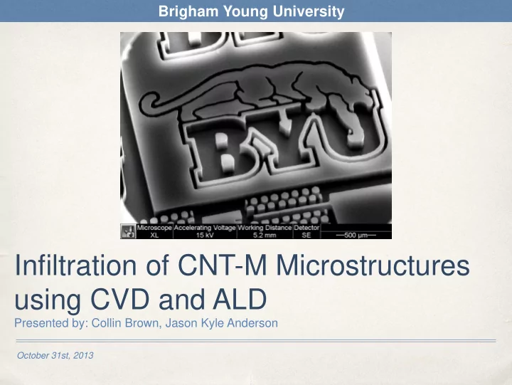

Brigham Young University Infiltration of CNT-M Microstructures using CVD and ALD Presented by: Collin Brown, Jason Kyle Anderson October 31st, 2013
Brigham Young University Acknowledgments Jason Kyle Anderson for his help in getting the system to work Dr's David Allred, Richard Vanfleet, and Robert Davis for their help and direction in this project BYU Environment for Mentoring Grant (MEG) Richard Hansen for his work on CNT-M David McKenna for constructing the CVD system
Brigham Young University Outline ✤ Purpose of Deposition Techniques ✤ Overview of CNT-M ✤ Theory of Deposition ✤ Chemical Vapor Deposition (CVD) ✤ Atomic Layer Deposition (ALD) ✤ Conversion of CVD system to ALD ✤ Initial Results ✤ Initial Characterization with SEM, TEM, and XEDS
Brigham Young University Purpose ✤ Create mechanical and electrical components on a micro scale - NEMS/MEMS
Brigham Young University Why does this matter? High sensitivity inertial sensors X-ray collimator (1) http://www.ducksters.com/games/ (2 wii-sports-bowling.php )
Brigham Young University Traditional Fabrication Method Etching- Chemically or mechanically removing selective parts of a solid metal (3)
Brigham Young University Limitations of Chemical Etching ✤ Limited selection of materials - Tungsten, Gold, Silicon, Aluminum ✤ Poor aspect ratio (height to width) (4 ✤ (~5:1) aspect ratio due to gas ) transportation limits
Brigham Young University New Method for NEMS/MEMS ✤ Carbon Nanotube Templated Micro-fabrication (CNT- M) ✤ Easily Controlled ✤ High Aspect Ratio (200:1) ✤ features >500 microns tall by 2-3 microns across ✤ Electrically conductive
Brigham Young University CNT-M Hot Ethylene Process Mask Photoresist Silicon Wafer
Brigham Young University Chemical Vapor Deposition (CVD) ✤ When used to infiltrate a CNT, called Chemical Vapor Infiltration (CVI) ✤ Flow reactants into chamber constantly, usually at high temperature ✤ Heat the solid precursor so it will volatilize ✤ Flow an inert gas to carry the precursor to the sample ✤ Problems ✤ Uneven Infiltration ✤ Capping
Brigham Young University (6) Before After infiltration infiltration Carbon Nanotube Forest Infiltrated with Forest - 1% Carbon Mo(CO) 6 by Richard Hansen
Brigham Young University
Brigham Young University
Brigham Young University
Brigham Young University
Brigham Young University Atomic Layer Deposition (ALD) ✤ Propose to try with Tungsten in nanotube forests, so Atomic Layer Infiltration (AFI) ✤ Self-limiting layer by layer ✤ Hope to achieve: ✤ uniform material properties ✤ eliminate crusts
Brigham Young University Tungsten ALD with WF 6 ✤ Gaseous form of WF 6 self-limits deposition ✤ Flow H 2 , monatomic Hydrogen from Plasma, or Silane ( SiH 4 ) ✤ H reduces WF 6 leaving a layer of W ✤ HF gas molecules created H 2 Vacuum Chamber Ar Sample WF 6 HF WF 6 W
Brigham Young University Converting the System ✤ Modified from CVD ✤ Hooked in gas lines for WF 6 ✤ Seal cabinet,install cabinet exhaust system, and insert sensors and filters for HF. ✤ Automate Labview TM program to cycle valves for ALD
Brigham Young University
Brigham Young University Initial Results
Brigham Young University
Brigham Young University Plasma - RF generated
Brigham Young University Latest Deposition - Pseudo ALD ✤ Constant H (40 sccm) - from a Hydrogen Plasma ✤ 5 seconds of WF 6 (0.0142 l at 5 psi, about 2.0 x 10 -4 mole) ✤ 120 cycles ✤ 235 degrees C - sample temperature ✤ Ozone treated 1 of the samples for 20 min, for better nucleation
Brigham Young University Ozone treatment vs No Ozone treatment ✤ 7 Ozone No Ozone Treatment Treatment
Brigham Young University Top of Side of Sample Sample
Brigham Young University Image of Fresh Surface from Top of Sample - Break in Lower Left Break
Brigham Young University No obvious difference between chemical makeup of small or large stuff
Brigham Young University ✤ scattered peaks have a lattice spacing too large for BCC tungsten ✤ may be an A15 compound, something like Beta-Tungsten
Brigham Young University Future Plans ✤ Optimize procedure (Intervals, flow rates, etc.) ✤ Silane vs. Hydrogen ✤ Ozone treatment vs. No Ozone treatment vs. In Situ Ozone treatment ✤ Annealing ✤ Characterization by SEM & TEM cross sectioning, Also X-ray characterization at ALS, FIB ✤ Capping ✤ Grain size uniformity ✤ Electrical conductivity ✤ Mechanical Properties
Brigham Young University Sources 1. http://www.memx.com/ 2. Johnson, R. Colin. “MEMS finds niche in space exploration.” EE Times, Sep 2007. <http://www.eetasia.com/ART_8800479803_1034362_NT_ca7d6a67.HTM>. 3. http://www.finestengraving.com/services.htm 4. Oxford Instruments. “Plasma Technology.” Accessed March 7, 2013. <http://www.oxfordplasma.de/process/arde.htm>. 5. Kellen Moulton, Nicholas B. Morrill, Adam M. Konneker, Brian D. Jensen, Richard R. Vanfleet, David D. Allred, and Robert C. Davis. “Effect of Iron Catalyst Thickness on Vertically Aligned Carbon Nanotube Forest Straightness for CNT- MEMS.” Journal of Micromechanics and Microengineering 22 (5) 055044. May 2012 and references cited therein. 6. Hansen, Richard Scott. "Mechanical and Electrical Properties of Carbon-Nanotube-Templated Metallic Microstructures." Senior Thesis. June 2012.
Recommend
More recommend