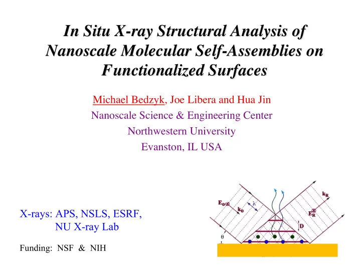

In Situ X-ray Structural Analysis of In Situ X-ray Structural Analysis of Nanoscale Molecular Self-Assemblies on Nanoscale Molecular Self-Assemblies on Functionalized Surfaces Functionalized Surfaces Michael Bedzyk, Joe Libera and Hua Jin Nanoscale Science & Engineering Center Northwestern University Evanston, IL USA X-rays: APS, NSLS, ESRF, NU X-ray Lab Funding: NSF & NIH
Outline: 1. Review experimental approach for X-ray analysis of layer-by-layer molecular assembly on functionalized surfaces: 2. Examples: a.) RNA adsorbed to amine terminated Self-Assembled Monolayer b.) Porphyrin-based nanoporous molecular films c.) Functionalized SAM attached to H-passivated Si(111) d.) In situ analysis of RNA adsorbed to charged surface
Experimental Approach Thin Film Characterization X-ray Tools: • X-ray Reflectivity (XRR) e - density profile, thickness & interface roughness • X-ray Fluorescence (XRF) Composition, Heavy atom coverages • X-ray Standing Waves (XSW): Heavy atom density profile Also study same samples with AFM and XPS
X-ray Vision Pros: Weak interaction with matter High penetrating power --> In situ analysis ---> buried structures Non destructive Atomic-scale resolution Advanced Photon Source Cons: Weak interaction with matter Need very intense X-ray source --> Synchrotron X-ray Source
Some X-ray Basics: Wave Property -> Structural Info λ = 0.1 to 10 Å wavelength E-M radiation X-rays scatter coherently from electrons Particle Property -> Compositional Info E γ = 1 to 100 keV energy Photo effect: Inner shell (K, L) ionization XRF energy spectrum: Decay of excited ion to ground state by characteristic XRF emission
Some X-ray Basics: (continued) Optics : Index of refraction: n < 1 for x-ray frequencies Snell’s Law: n 1 cos θ 1 = n 2 cos θ 2 --> Total External Reflection (TER) of X-rays θ 2 = 0 --> TER --> θ 1 = θ C (critical angle) θ C = (2 δ ) 1/2 , where n=1- δ , δ ~ N e Eg. Si at λ = 1.54 Å, δ = 7.4 x 10 -6 , θ C = 3.9 mrad = 0.22° θ 1 θ 1 θ 2 TER -> Evanescent Wave Effect
X-Ray Reflectivity Analysis Example: SAM / Si(111) XRR data and fit 0 10 l e d o -2 10 m b a l -4 s 10 Reflectivity Reflectivity 1 -6 H-Si H-Si 10 -8 10 SAM-1 SAM-1 -10 10 SAM-2 SAM-2 -12 10 0 0.1 0.2 0.3 0.4 0.5 0.6 0.7 - 1 - 1 q (Å q (Å ) q = 4 π sin θ / λ , reciprocal space coord. Fresnel Theory: R~ 1 for q < q C = 0.031 Å -1 Si mirror TER R F = (2q/q C ) -4 for q>>q C . Fourier transform of a step function.
X-Ray Reflectivity Analysis Example: SAM / Si(111) XRR data and fit 0 10 l e d o -2 10 m b a l -4 s 10 Reflectivity Reflectivity 1 -6 H-Si H-Si 10 -8 10 SAM-1 SAM-1 -10 10 SAM-2 SAM-2 -12 10 0 0.1 0.2 0.3 0.4 0.5 0.6 0.7 - 1 - 1 q (Å q (Å ) •At 1 st dip, the 2 scattered plane-waves from the top and bottom interfaces have a λ /2 path-length difference (or π phase difference). •Modulation period -> film thickness Range: 1 to 100 nm •Modulation Amplitude -> relative electron density of film •Modulation damping -> roughness of interface(s) Range: < 2 nm
X-Ray Reflectivity Analysis Fundamentals 2 R ( q ) = R F ( q ) | Φ ( q ) | Kinematical approach: q = 4 π sin θ / λ Φ ( q ) = 1 d ρ iqz dz e ∫ θ θ dz ρ ∞ R ( q ) 1 slab 2 e 2 2 σ − q − iqt R F ( q ) = (1 − b ) + be model ρ = e - density, b = ρ F / ρ Si, σ = σ s = σ I = (rms) roughness, t = film thickness Dynamical approach: Parratt’s recursive formulation
X-ray Standing Wave Fundamentals Superposition of 2 Plane-Waves E T = E 0 e 2 π i ( K 0 • r − ν t ) + E R e 2 π i ( K R • r − ν t ) SW Intensity: 2 I = E T = I 0 + I R + 2 I 0 I R cos( v − 2 π Qz ) SW Period: D = 1 λ = Q 2sin θ SW Vector: Q = K R − K 0
X-ray Standing Wave Generated by Reflection λ XSW Period: D = 2sin θ I max − I min Fringe Visibility: V = I max + I min XSW Generated by Strong Reflection: R=1 → V = 1 1. Dynamical Bragg Diffraction: D = d-spacing a) Single crystal d = 1 to 10 Å surface structure b) Multilayer (LSM) d = 20 to 200 Å ultrathin organic film 2. Total External Reflection: D = 70 Å to 1 µ m diffuse double-layer
XSW Generated by Dynamical Bragg Diffraction from Single Xtal I = I 0 [1 + R + 2 R cos( v − 2 π H • r )] H • r = Δ d d k k H 0 XSW XSW π phase shift → d/2 inward shift Low-angle side → Nodes on diffraction planes Hi-angle side → Antinodes on diffraction planes XSW Fluorescence Yield θ I ( θ , r ) ρ ( r ) d r Y ( θ ) = ∫ [ ] ( ) Crystal Y( θ ) = 1 + R( θ )+ 2f H R( θ )cos v( θ )-2 π P H d f H : Coherent Fraction: Amplitude: 0 --> 1 π 1 P H : Coherent Position: Phase : 0 --> 1 Phase v H th Fourier Comp. of the fluorescence-selected R atom distribution ρ ( r ). 0 0 Angle θ
XSW analysis of strain in a buried heteroepitaxial film Can measure strain down to the level of 1 atomic layer. HRXRD needs > 10 layers Ge K α Si K α Si cap Si(001) 1 ML Ge Cap Ge layer Si(001) Si(001) Substrate substrate [001] ε ⊥ = − 2 c 12 ε || c - [110] 11 [110]
X-Ray Experimental Setup X-Ray Experimental Setup 5ID-C, DND-CAT Advanced Photon Source, Argonne National Lab X-ray detector Fluorescence slits Solid-state fluorescence detector Horizontal focussing mirrors Sample Slits e - Ion chambers Synchrotron ring LN -cooled Si(111) 2 double crystal monochromator Undulator DuPont-Northwestern-Dow Collaborative Access Team
Total External Reflection Total External Reflection X-ray Standing Waves X-ray Standing Waves n = 1 n = 1 - δ - i β z = 0 Fresnel Theory : θ − θ 2 − 2 δ − 2 i β 1/ 2 ( ) E R = E R e iv = z = 2D C θ + θ 2 − 2 δ − 2 i β 1/ 2 E 0 E 0 ( ) R E − Field Intensity : ( ) = 1 + R + 2 R cos ν − 2 π Qz ( ) I θ , z ν Q = 2sin θ λ Critical Period : Normalized Incident Angle - θ / θ C 80Å for Au D C = λ π = = 2 θ C 2 r e N e 200Å for Si
LB Multilayer Film / Au Mirror Wang, Bedzyk, Penner, Caffrey Nature (1991). Raw TER-XSW Data Zn K α ZnA R x4 2 ω TA 160 Å Au Zn Fluorescence Yield ZnA 8 ω TA 500 Å Au ZnA 14 ω TA 900 Å Au Y( θ )= ∫ ρ (z) I( θ ,z) dz Angle θ (mrad)
Multilayer X-ray Mirror -> Nanometer Variable Period XSW • Si / Mo Layered -Synthetic Microstructure made by DC magnetron sputtering • Large d-spacing (d = 22 nm) provides XSW periods of D = 5 - 20 nm • Top Si surface w/ native oxide SiO x supports primer layer for self-assembly Hg Hg Hg Hg Hg Hg Hg _ _ 20.0 _ _ _ _ _ _ _ _ _ + + + + + + + + + + + D xsw = NH 3 NH 3 NH 3 NH 3 NH 3 NH 3 NH 3 NH 3 NH 3 NH 3 NH 3 13.0 nm 8.9 Si/Mo 6.4 multilayer x-ray mirror Si substrate 5.1 12.4 keV @NSLS/x15a Nov. 2002
Simple Test Case Evaluation of Variable Period XSW Hg modeled as a 0.5 nm thick Hg Hg Hg Hg Hg Hg Hg _ _ slab at the substrate surface Hg-polyU _ _ _ _ _ _ _ _ _ + + + + + + + + + + + NH 3 NH 3 NH 3 NH 3 NH 3 NH 3 NH 3 NH 3 NH 3 NH 3 NH 3 Si/Mo multilayer x-ray mirror Si substrate 12.4 keV @NSLS/x15a Nov. 2002
Hg modeled as slab on top of NH 3 + layer 4 t = 0.5 nm Hg L α Fluorescence Yield (CPS) 2 t = 10 nm 3 1.5 2 1 1 Reflectivity 0 0.5 -1 0 -2 0.02 0.04 0.06 0.08 0.1 0.12 Q (1/Å) 12.4 keV @NSLS/x15a Nov. 2002 RNA is laying flat down on surface, not coiled
Mercurated Poly U The RNA molecule → mercurated Poly-uridylic Acid Potassium salt • Molecular weight: 1,400,000 - 1,700,000 • link number: 2382 - 2905 o C 9 N 2 O 8 H 9 KPHgCl HgCl Cl Hg Cl Hg Cl Hg H (Hg replaced H) (Hg replaced H) O N H N Unit weight: 579.28 o CH 2 O P O O Concentration: 47 µ g/mL H H O- H H K+ one Hg atom per units OH
X-ray Nanoscale Profiling of Layer-by-Layer Assembled Metal/Organo-Phosphonate Films Libera, Gurney, Nguyen, Hupp, Liu, Conley, Bedzyk Langmuir (2004) 4 Hf O O • Nanoporous molecular thin films based on Porphyrin single- and multi-layer O P molecular membranes. Developed for R 3 biological sensor application. • Self-assembly using the metal- O P phosphonate scheme. Zr O O 2 Zr • X-ray characterization of Films 1. (a) thickness and density - XRR O O 1 2. (b) z atom-profile of metal atom O P layers - XSW 3. (c) areal packing density by R = alkane chain coverage measurements - XRF = porphyrin = porphyrin square
XSW Analysis of 8 Layer Porphyrin Film 20.0 nm Y (a) Zr z 0 =0.8 nm σ =0.4 nm Por. ρ Zr C Zr = 0.8 Hf Por. Normalized Fluorescence Yield Hf 2 Por. C Y = 0.6 ρ Y 1 (b) Y z 0 =18.5 nm σ =0.8 nm Hf 2 1 Por. 19 Hf Por. (c) Hf Hf ρ Hf C Hf = 1.0 Por. 1 18 Hf C Hf = 0.0 Por. 2.5 nm Hf Por. Reflectivity 0 nm Zr SiO 2 surface (d) Si Mo q ( Å -1 ) Si/Mo multilayer substrate
X-ray E-field Intensity Surface for sample A8 t ( ) ( ) dz XSW Fluorescense Yield : Y ( θ ) = I θ , z ρ z ∫ 0 ( ) = distributionof fluorescent species ρ z distance above substrate - nm E-field Intensity i n c i d e n t a n g l e - m r a d resonant cavity E-field enhancement EFI > 4
Recommend
More recommend