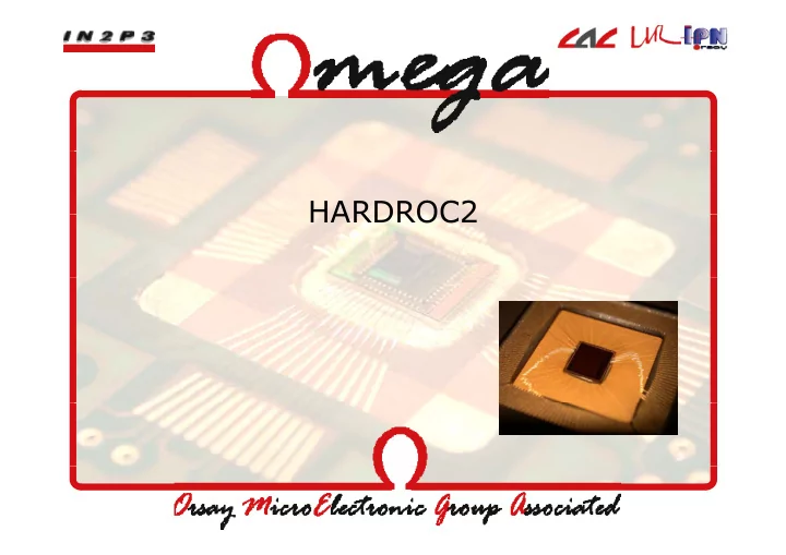
HARDROC2 HARDROC2 HARDROC2 Hardroc2 submission: mid june 08, - PowerPoint PPT Presentation
HARDROC2 HARDROC2 HARDROC2 Hardroc2 submission: mid june 08, Hardroc2 submission: mid june 08, Delivered end of october 08: 6 packaged chips, 440 naked dies Package: QFP160 1single row of pads 4.7 mm 28 mm 3mm 4.3 2
HARDROC2 HARDROC2
HARDROC2 • Hardroc2 submission: mid june 08, Hardroc2 submission: mid june 08, • Delivered end of october 08: 6 packaged chips, 440 naked dies • Package: QFP160 1single row of pads 4.7 mm 28 mm 3mm 4.3 2 Plastic (Thin QFP): 1.4 mm 28 mm (C (Ceramic: 3.4 mm) i 3 4 ) HR2 status,CALICE meeting,DAEGU, KOREA, 18 Feb 09, NSM 2
HARDROC2: HARDROC1 +modifs • Dynam ic range extension y g – Gain correct.: 8 bits instead of 6: G=0 to 255 (analog G=0 to 2) – 3 shapers, different Rf,Cf and 3 shapers, different Rf,Cf and gains : • Fsb1, G= ½, 1 / 4 ,1/8,1/16 • Fsb2, G= 1/8, 1 / 1 6 ,1/32,1/64 – 3 thresholds (=> 3 DACs): • 10 fC, 100fC, 1pC (megas) • 100fC, 1pC, 10pC (GRPC) • Correction of the minor bugs of HR1 : MASK, memory pointer (dummy frame) • 8 7 2 SC registers , default config • Pow er pulsing: p g – Bandgap (redesigned)+ ref Voltages + master I: power pulsed – POD module (power budget) POD module (power budget) HR2 status,CALICE meeting,DAEGU, KOREA, 18 Feb 09, NSM 3
SC/Read pb • To spare output PADS and to avoid parasitics on the To spare output PADS and to avoid parasitics on the Di it l SW Digital SW SC registers, SELEC + switch to deliver: – sr_sc, clk_sc, rstb_sc Slow rstb_read – sr_read, clk_read, rstb_read control Data sr rstb _ input input Probe rstb_sc – Pb=digital sw and reset active low => reset of the SC registers when SELEC switched on the read selec Select register • Read register not essential but usefull for debug and characterisation => Focused Ion Beam on 2 packaged chips to be able to use the Read register • SC loading: – 872 SC parameters – Vddd=4V necessary to load some SC config y g strap HR2 status,CALICE meeting,DAEGU, KOREA, 18 Feb 09, NSM 4
3 10bit-DACs • DAC0 : fine= > -1 .1 m V/ UDAC / – Vmax Vmin std – 2.3268 1.9966 0.09 • DAC0 : coarse = > -2 .2 1 m V/ UDAC DAC0 : coarse > 2 .2 1 m V/ UDAC – Vmax Vmin std – 2.3271 1.66379 0.192 • DAC1 : coarse = > -2 .0 6 m V/ UDAC DAC1 : coarse > 2 .0 6 m V/ UDAC • DAC2 : coarse = > -2 .1 2 m V/ UDAC HR2 status,CALICE meeting,DAEGU, KOREA, 18 Feb 09, NSM 5
FSB measurements <>dc fsb: Independant of G Pedestal= 90 ±2 <>=2.14V = pedestal equiv. to DAC0 (coarse) ≈ 90 G=256 G=256 G=0 FSB0 , 1 0 0 fC injection, G= 1 2 8 : optim um Signal/ Noise ratio All swi ON All i ON 70 70mV, V σ =750µV 750 V S/N S/N=93 93 tp=23ns Sw_150fF on 203 mV 1.2mV 168 Sw_100fF on 243 mV 1.3 mV 187 Sw_100k and sw_100fF on 153 mV 930 µV 165 Sw_50fF on 100 mV 1.5 mV 67 No swi on (=> internal 20fF, 421 mV 1.8 mV 233 100k 100k only) l ) HR2 status,CALICE meeting,DAEGU, KOREA, 18 Feb 09, NSM 6
Waveforms and Xtk: scope measurements FSB0, Qinj=100fC Xtk x10 FSB1 (0100), Qinj=1 pC FSB0 normalised to 1 FSB2 (0100), Qinj=10 pC Analog Xtk < 1% Testboard wo any decoupling cap. HR2 status,CALICE meeting,DAEGU, KOREA, 18 Feb 09, NSM 7
Digital Xtk (board wo DECOUPLING CAP) • Coupling of the discri output to the FSB output of the direct li f h di i h f h di neighbors HR2 status,CALICE meeting,DAEGU, KOREA, 18 Feb 09, NSM 8
Digital Xtk measurements (board wo DECOUPLING CAP) • ch39 ch39 FSB0 ( sw _ Cf= 1 0 0 fF, sw _ Rf= 1 0 0 k and ( f f f k d ch41 G= 1 4 4 ) : • 1 0 0 fC in ch4 0 , Vth0 = 2 0 5 = > 2 0 0 m V, trigger for Vth0 < 2 0 5 trigger for Vth0 < 2 0 5 • Qinj= 1 pC ( 1 V@2 0 dB in 1 0 pF) , no trigger on direct neighbours ch38 • Qinj> 2 .5 pC ( fsb0 sature) , trigger on ch3 9 and ch4 1 ie 4 % ch4 1 ie 4 % • Qinj> 7 pC ( fsb0 sature) , trigger on ch3 8 ,3 9 and 4 1 ,4 2 ch40 • Qinj> 5 6 pC, triggers on 3 7 ,3 8 ,3 9 and 4 1 ,4 2 • 1 0 0 pC, triggers on ch 3 4 ,3 5 ,3 6 ,3 7 ,3 8 ,3 9 and 1 0 0 pC, triggers on ch 3 4 ,3 5 ,3 6 ,3 7 ,3 8 ,3 9 and ch 4 1 ,4 2 ,4 3 ,4 4 ,4 5 ,4 6 • • FSB1 ( 5 0 f,1 0 0 fF,1 0 0 k,5 0 k and G= 1 4 4 and Gnm os= 1 0 0 0 ) : FSB1 ( 5 0 f,1 0 0 fF,1 0 0 k,5 0 k and G= 1 4 4 and Gnm os= 1 0 0 0 ) : • 1 pC, Vth1 = 4 4 3 = > 7 3 0 m V, trigger for Vth1 < 4 4 5 • Qinj= 1 pC ( 1 V@2 0 dB in 1 0 pF) , no trigger on direct neighbors • Qinj> 5 6 p, trigger on ch3 9 and 4 1 • 1 0 0 pC, triggers on ch3 9 and ch 4 1 • FSB2 ( 5 0 f,1 0 0 fF,1 0 0 k,5 0 k and G= 1 4 4 and Gnm os= 0 0 1 0 ) : • 1 0 pC, Vth2 = 2 3 0 = > 7 3 0 m V, trigger for Vth2 < 2 3 3 • Qinj= 1 pC ( 1 V@2 0 dB in 1 0 pF) , no trigger on direct neighbors Qi j 1 C ( 1 V@2 0 dB i 1 0 F) t i di t i hb • Qinj= 1 0 0 pC, no triggers on neighbours HR2 status,CALICE meeting,DAEGU, KOREA, 18 Feb 09, NSM 9
8bit PMOS MIRRORS: linearity measurement Vout Vout Qinj=100fC •Allows accomodating the gain according to the detector choice •PMOS gain: 8 bits/channel •Binary G b = 0 to 255 •Analog G = 0 to 2 g •Current mirrors mismatch between channels (small size transistors to optimise the speed): ( p p ) layout redone in HR2 to improve the uniformity HR2 status,CALICE meeting,DAEGU, KOREA, 18 Feb 09, NSM 10
FSB0 scurves: HR1 /HR2 before and after gain correction HR1 before cor. HR2 before cor. HR2 before cor. Qinj=100fC Qinj 100fC HR1 after cor. HR2 after cor. Pedestal substracted 1.4% 9% 6.7% 5% HR2 status,CALICE meeting,DAEGU, KOREA, 18 Feb 09, NSM 11
SCURVES: FSB0,1,2 • Gain=144 for all channels before correction Gain 144 for all channels before correction • Gain correction performed for each channel on FSB0, not efficient on FSB1 and FSB2 as non uniformity is dominated by non uniformity of NMOS mirrors used to change Gnmos In GREEN= after gain correction g 6 7% 6.7% 1 3% 1.3% 7% 6% FSB0 , 100 fC FSB2 , 1pC 5 5% 5.5% 5% 3% FSB1 , 1pC FSB2 FSB2 , 10pC 10pC HR2 status,CALICE meeting,DAEGU, KOREA, 18 Feb 09, NSM 12
POWER CONSUMPTION • • Maximum power available: Maximum power available: PA 5.46mA DAC 0.84mA – 10 µW/ch with 0.5% duty cycle 3 FSB 12.3mA BG 1.2mA – => 640µW/3.5V=180 µA for the entire chip entire chip vddd ddd 0 67mA 0.67mA 9 3mA 9.3mA SS SS – OFF= Ibias _cell switched off 3 Discris 7.3mA vddd2 0.4mA during interbunch (=0 if 40MHz – SW added in HR2 to switch off OFF) OFF) all the master Ibias, Vref, 38mA TOTAL V_BG… Pwr_on_a alone (FSB0 14.9mA and discri0 ON only) Pwr_on_dac 1.025mA Pwr_on_d 0.93mA • ALL ON 17 mA Without SS: – 38-9=29mAx3.3V ≈ 100mW ALL OFF < 4 µA – 1.5mW/ch – 7 5 µW/ch with 0 5% duty cycle 7.5 µW/ch with 0.5% duty cycle HR2 status,CALICE meeting,DAEGU, KOREA, 18 Feb 09, NSM 13
Power pulsing of HR2: « Awake » time PWR ON PWR ON PWR ON FSB0 25 µs 8 µs • PWR ON: ILC like (1ms,199ms) • Trigger All decoupling capacitors removed • PP of the analog part: – Input signal synchronised on PWR ON – => Awake time= 8 µs DAC output (Vth) • Power pulsing of the DAC: – 25 µs (slew rate limited) HR2 status,CALICE meeting,DAEGU, KOREA, 18 Feb 09, NSM 14
Power On Digital module (POD) POD module StartLVDS • • PowerON start/stop clocks and PowerON start/stop clocks and LVDS receiver bias current to Clkin LVDS ClkOut Receiver meet power budget. Enable Clock • LVDS receivers for f for Acquisition and A i i i d PowerOnDigital Conversion EnableClock RazChn/NoTrig and ValEvt ON Enable Clock StartReadOut for during PowerOnAnalog (during du g o e O a og (du g Rstb StartReadOutInt Clkin Readout Enable Enable bunch crossing) ClkOut EndReadOut • Clock is started Phases Acquisition Conversion Readout (99% time) asynchronously, enabled and h l bl d d PowerOnInt stopped synchronously (at ‘0’) Chip 1 • 2 operation modes : p PowerOnInt Chip 2 – Acquisition, Conversion � PowerOnInt common to all managed by Chip N DAQ DAQ – Readout � daisy chained managed by StartReadOut and • POD successfully tested on EndReadOut EndReadOut testbench HR2 status,CALICE meeting,DAEGU, KOREA, 18 Feb 09, NSM 15
CONCLUSION • • HR1 bugs corrected ( Mask memory pointer) HR1 bugs corrected ( Mask, memory pointer) • 0.5% duty cycle pwr pulsing: pwr <8µW per channel • Better uniformity between channels before correction: 7%, y , down to 1.5% (fsb0) after correction (that might be not necessary for RPC) • • Scurves@ 1pC and 10 pC OK dispersion=5% Scurves@ 1pC and 10 pC OK, dispersion=5% HR2: operates in full I LC m ode and is suitable for m 2 ( No • ( p analog output) and production when validated on detectors. • 400 HR2 400 HR2 are in I2A packaging company (USA) to be i I2A k i (USA) t b packaged in plastic TQFP160. • Must be TESTED (=characterisation=>30minutes/chip) ( p) • Power pulsing tested on testbench. To be tested in test beam • Datasheet available on http:/ / om ega.in2 p3 .fr h il bl h / / i f HR2 status,CALICE meeting,DAEGU, KOREA, 18 Feb 09, NSM 16
ANNEX HR2 status,CALICE meeting,DAEGU, KOREA, 18 Feb 09, NSM 17
Recommend
More recommend
Explore More Topics
Stay informed with curated content and fresh updates.
