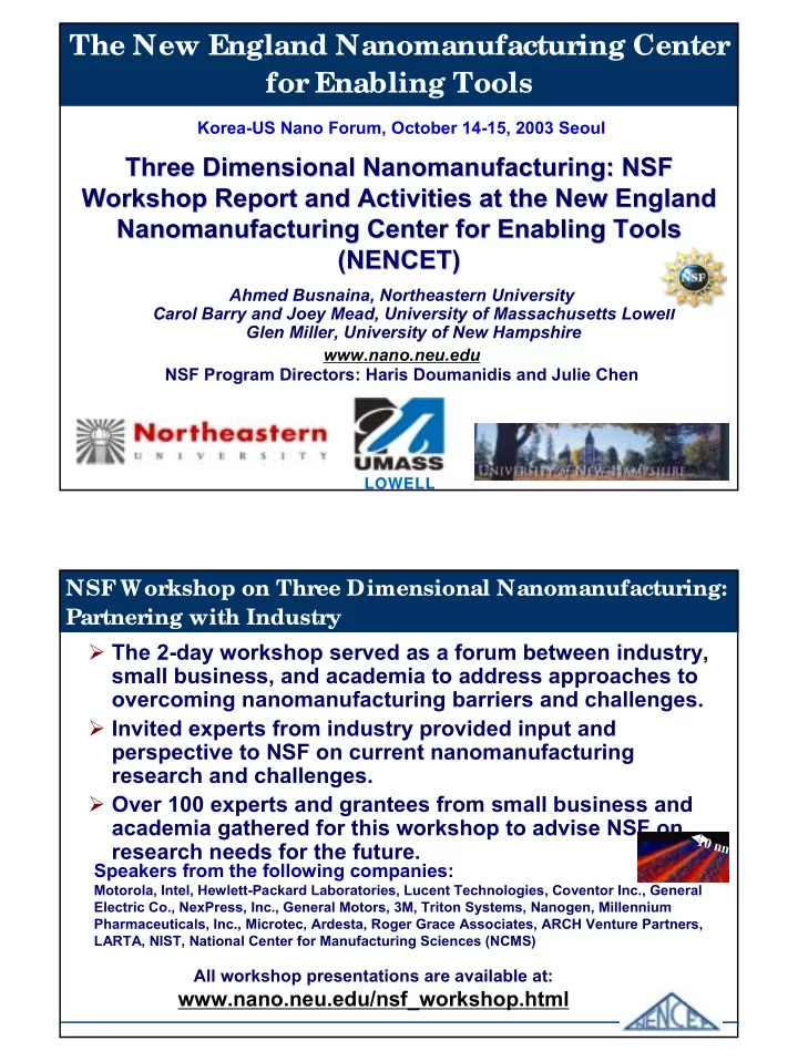

The New England Nanomanufacturing Center “ for Enabling Tools Korea-US Nano Forum, October 14-15, 2003 Seoul Three Dimensional Nanomanufacturing: NSF Three Dimensional Nanomanufacturing: NSF Workshop Report and Activities at the New England Workshop Report and Activities at the New England Nanomanufacturing Center for Enabling Tools Nanomanufacturing Center for Enabling Tools (NENCET) (NENCET) Ahmed Busnaina, Northeastern University Carol Barry and Joey Mead, University of Massachusetts Lowell Glen Miller, University of New Hampshire www.nano.neu.edu NSF Program Directors: Haris Doumanidis and Julie Chen LOWELL LOWELL NSF Workshop on Three Dimensional Nanomanufacturing: Partnering with Industry � The 2-day workshop served as a forum between industry, small business, and academia to address approaches to overcoming nanomanufacturing barriers and challenges. � Invited experts from industry provided input and perspective to NSF on current nanomanufacturing research and challenges. � Over 100 experts and grantees from small business and academia gathered for this workshop to advise NSF on 10 nm research needs for the future. Speakers from the following companies: Motorola, Intel, Hewlett-Packard Laboratories, Lucent Technologies, Coventor Inc., General Electric Co., NexPress, Inc., General Motors, 3M, Triton Systems, Nanogen, Millennium Pharmaceuticals, Inc., Microtec, Ardesta, Roger Grace Associates, ARCH Venture Partners, LARTA, NIST, National Center for Manufacturing Sciences (NCMS) All workshop presentations are available at: www.nano.neu.edu/nsf_workshop.html
Panel and Attendee Input � What is the current state of the art? � Where are we headed? � What are the barriers? � Technical � Cultural/Infrastructure � What should be done to help accelerate nanomanufacturing success? What is the Current State of the Art? Commercial Products GM: Thermoplastic nanocomposites for automotive components Triton: Nanocomposite air pouch for athletic shoes, packaging, and chemical-biological protective clothing M-Van Step Assist 3M: CMP fixed micro fabricated abrasive pad
What is the current state of the art? Products in Progress � HP: High density (6.4 Gbit/cm 2 ) electronically addressable memory (Molecular Switch Crossbar Circuits) � Intel: Nano-transistors for logic technology � Lucent: Rubber stamps and plastic circuits for electronic paper (plastic or paper display) � Lucent: 3D microfabrication via printing on curved objects � Lucent: Large area nanoreplication with a flexible PNAS, 98 (9), 4835 (2001) mold Science , 291 , 1502 (2001) � Motorola: Nano elements of an OFET � Triton: Nanoparticles cancer therapy � Triton: Organic electronic materials Possible Products; Nanotube Memory Chip 1000 Nanotube memory Chip goal Cell Density (Gbit/cm 2 ) 2 100 DARPA goal (2004) HP molecular switch Application 10 • Nanotube sw itch based storage device capable of 3 - 5 orders of m agnitude m ore storage than today’s devices 1 Requires Current CMOS • Massive precise parallel assem bly of CNTs “red brick wall” 0.1 2001 2004 2007 2010 2013 2016 Year of DRAM Introduction
Example of Work in Progress; Molecular Electronics, HP Utilizes Sw itchable Molecules • I t’s sm all • I t functions Roxtaxane • I t’s cheap F. Stoddart, UCLA Nanoscale Molecular Devices Pt Pt Ti SiO 2 /Si US Patent# 6407443
Nanoscale Molecular Devices Pt Ti Pt US Patent# 6407443 Molecular Crossbar Circuits 1 µ m 100 nm 100 µ m 10 µ m 1 mm
Where are we headed? � Development of processing methods for fabrication of nanomaterials � New materials with unique properties � Environmentally friendly nanomanufacturing processes � Process models Pt � Heterogeneous, multi-scale materials/device integration and assembly. SiO 2 4 0 n Ti/Pt m What are the barriers? Technical � Assembly of 3D heterogeneous systems � Low rates of 3D manufacturing � Alignment and registration - multilayers and interconnects � Interconnection at three dimensions, various length scales, different materials, and functionalities � Packaging � Quality � Low reliability and yield are key issues for nanoscale devices that need to be solved � Reproducibility and repeatability of nanomanufacturing � Control of contamination and development of fault /defect tolerant devices � Control of morphology to produce an engineered structure.
What are the barriers? Technical � Modeling � Limited understanding of fundamental physics � Lack of component specifications, material specifications, reliability models, simulation models � Materials � Cost and availability of materials for scale up � Metrology of nanodevices � Lack of real time characterization methods � Requirement for manufacturing processes that are robust under commercial environments (not Class 1 clean rooms) What are the barriers? Cultural/Infrastructure � Infrastructure � Lack of standards, instrumentation, and tools � Lack of affordable infrastructure (facilities, equipment, design tools, skilled personnel) � Lack of nanotechnology roadmaps � Cultural � Limited knowledge of nanomanufacturing processes within traditional manufacturing community � Education needed for both scientists and engineers � IP issues � “Nano-fear ”
How to accelerate nanomanufacturing success? � Funding and Resources � Spread roles, risks, and rewards among industry, academia, and government, motivate & reward risk taking � Existing approaches � Government funding (e.g., GOALI, STTR, ATP projects) � Research centers of excellence programs at universities that include small and large business participation � Additional approaches � Support more applied academic researchers to bridge the gap to meet industrial needs � Government-Industry support of university associated incubator programs. � Expand national R&D infrastructure with not for profit applied research centers emulating CSEM or Fraunhofer Institutes. How to accelerate nanomanufacturing success? � Communication � Constant feedback and information dissemination between industry and academia � Creation of user groups � Workshops � Connecting small companies with VC (e.g., Matchmaker) � Integration between academia and industry � Education and clarification on IP issues � Exchange of industrial workers with faculty and students � Better consideration of technology scale-up issues by academia � Application focus required to accelerate development
The New England Nanomanufacturing Center “ for Enabling Tools Research Activities at the New England Research Activities at the New England Nanomanufacturing Center for Enabling Tools Nanomanufacturing Center for Enabling Tools (NENCET) (NENCET) Ahmed Busnaina, Northeastern University Carol Barry and Joey Mead, University of Massachusetts Lowell Glen Miller, University of New Hampshire LOWELL LOWELL Overcoming Barriers to Commercialization To move scientific discoveries from the � laboratory to commercial products, a ercoming Barriers to Commercializat completely different set of fundamental research issues must be addressed. Com m ercial Products Industrial Collaboration The field of nanomanufacturing is � Enabling Nanom anufacturing Tools incredibly broad, Reel- to- Reel Manufacturing, Molecular Tem plates, Accelerated Nevertheless, three critical and Life Testing, Process Design Tools � fundamental technical barriers to Assem bly High- Rate/ manufacturing surface repeatedly: Reliability and Volum e and Connectivity Processing Testing (1) Smart t ooling (guided self - Barriers to Nanomanufacturing assembly using nano t emplat es) and wiring Thrust 1 Thrust 2 Thrust 3 (2) High- rat e/ high- volume Current Nanoscience Knowledge Base processing. (3) Reliabilit y and t est ing
Nanotube Memory Chip � Potential $100 billion market � Non-volatile memory � Nanotube based storage device capable of 3-5 orders of magnitude more storage � Memory accessible at orders of magnitude faster 2 than silicon chips. � Breakthroughs needed for: � Large-scale precise, economic assembly of CNTs � with specific orientation and functionality � with connection to the micro/macro level � at high rate and volume Other SWNT Scientific Roadblocks: ► One size does not fit all where applications are concerned ► Structure-property relationships unknown. How do properties vary as a function of precise molecular dimensions? ► Lack of Solubility ► Organic Chemistry of SWNTs, Lack of chemical functionality How Can Nano Templates Be Used To Assemble Nanoelements (SWNT, DNA, Nanorods)? 2. Nanotubes align 1. Electrostatically on negatively addressable nanowires charged nanowires via noncovalent, electrostatic attraction self-ordering growth - + - - of nanowires on - - + + + - strained interfaces 3. A new stronger Substrate is attractive brought with interactions a few nano- meters 4. Nanotube transfer is complete
Recommend
More recommend