Fascinated Journeys into Blue Light Isamu AKASAKI Meijo University - PowerPoint PPT Presentation
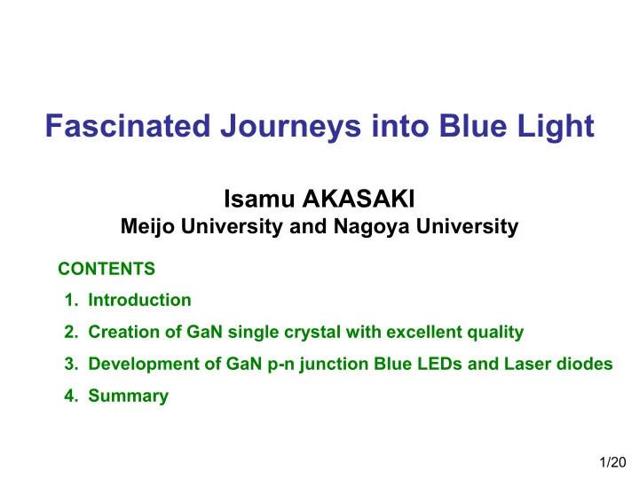
Fascinated Journeys into Blue Light Isamu AKASAKI Meijo University and Nagoya University CONTENTS 1. Introduction 2. Creation of GaN single crystal with excellent quality 3. Development of GaN p-n junction Blue LEDs and Laser diodes 4.
Fascinated Journeys into Blue Light Isamu AKASAKI Meijo University and Nagoya University CONTENTS 1. Introduction 2. Creation of GaN single crystal with excellent quality 3. Development of GaN p-n junction Blue LEDs and Laser diodes 4. Summary 1/20
1. Introduction 2/20 Blue Light-Emitting Devices (LED, Laser diode) [ A ] Energy bandgap Eg : >2.6 eV (< 480 nm) (Wide bandgap semiconductors) [ B ] Energy band structure : Direct-transition type for conservation of electron momentum Conduction band electron Energy bandgap Eg Electron energy Excitation Light light (radiative recombination) (Positive) hole Valence band (Internal) photo-electric effect spontaneous emission Conservation of energy
1. Introduction 3/20 High-performance Blue LED and Laser diode [1] High-quality single crystal [2] p-n junction Depletion layer n type p type - - - - - - - - - - - - - - - - + + + + + + + + + + + + + + + - - - - - - - - - - - - - - - + + + + + + + + + + + + + + + - - - - - - - - - - - - - - - + + + + + + + + + + + + + + + - - - - - - - - - - - - - - - + + + + + + + + + + + + + + + electron hole Electron energy - + Light emission Eg hole ( ~3V ) Applied forward voltage Electric current p-n junction LED p-n junction
1. Introduction 4/20 Candidate materials for Blue Light-Emitters in 1960s-’70s ZnSe GaN [A] Energy gap (Eg) 2.7 eV 3.4 eV [B] Energy band structure direct direct [1] Crystal growth straightforward too difficult Substrate GaAs sapphire Lattice mismatch 0.26 % 16 % [2] p-n junction not realized at that time few Number of researchers many Physical & chemical stability low high
1. Introduction 5/20 Candidate materials for Blue Light-Emitters in 1960s-’70s ZnSe GaN [A] Energy gap (Eg) 2.7 eV 3.4 eV [B] Energy band structure direct direct [1] Crystal growth straightforward too difficult Substrate GaAs sapphire Lattice mismatch 0.26 % 16 % [2] p-n junction not realized at that time few Number of researchers many Physical & chemical stability low high Chose GaN in 1973 at Matsushita Research Institute Tokyo ( MRIT ) because of toughness , wider direct Eg , and non-toxicity
1. Introduction 6/20 Started growth of GaN by MBE in 1973, and by HVPE in 1975 GaN MIS Blue LED by HVPE First as-grown highly n-type cathode SiO 2 film sapphire 1978 Epoxy dome h ν n-GaN n-GaN i-GaN (30 μ m) Ohmic MIS Blue LED i-GaN electrode (~1 μ m) The brightest Blue LED at that time, however, still weak and high operating voltage MIS Blue LED, not p-n junction LED at MRIT
1. Introduction 7/20 Potential of GaN at MRIT High-quality tiny crystallites 100 μ m Surface of GaN grown on sapphire by HVPE (1975-78) Tiny but high-quality crystallites embedded in HVPE-grown crystals Recognized the great potential of GaN Made up my mind to go back to the beginning; i.e. Crystal Growth in 1978
2. Creation of GaN single crystal with excellent quality 8/20 Crystal growth methods for GaN Hydride Vapor Phase Epitaxy (HVPE) H. P. Maruska and J. J. Tietjen: (1969). GaCl (g) + NH 3 (g) = GaN (s) + HCl (g) + H 2 (g) Issues: Susceptible to reverse reactions, Too fast growth rate Molecular Beam Epitaxy (MBE) I. Akasaki: (1974) (unpublished). 3 Ga (g) + NH 3 (g) = GaN (s) + H 2 (g) 2 Issues: Prone to nitrogen deficiency, Slow growth rate (at that time) Metalorganic Vapor Phase Epitaxy (MOVPE), (MOCVD) H. M. Manasevit et al: (1971). Ga(CH 3 ) 3 (g) + NH 3 (g) GaN (s) + 3CH 4 (g) Advantages: • No reverse reactions • Easy to control growth rate, alloy (AlGaN, GaInN) composition, and impurity-doping Decided to adopt MOVPE (1979) at MRIT
2. Creation of GaN single crystal with excellent quality 9/20 Started anew to MOVPE since 1981 at Nagoya University Improvements in MOVPE reactor and growth condition (1) (2) NH 3 +H 2 TMG+TMA+H 2 NH 3 +H 2 (1985) TMG+(TMA)+H 2 0.7~20cm/sec delivery tube Y. Koide Reactor substrate sapphire 110 cm/sec (1) guide susceptor RF coil Inclined substrate (2) Reactor design changed Exhaust Exhaust First MOVPE system (Handmade) 10 μ m Mixing TMG (TMA) with NH 3 just before the reactor inlet, and (1) High speed gas flow (2) Substrate inclined at a 45-degree angle GaN Suppressed the convective gas stream, and the adduct formation sapphire Bird-view Uniform growth, but not specular surface, still poor material quality SEM image by H. Amano
2. Creation of GaN single crystal with excellent quality 10/20 Growth on Growth on the same substrate a highly-mismatched substrate Interfacial energy σ defects GaN A A GaN mismatch GaN ~ 16% A B sapphire but not available Lattice Homoepitaxy Heteroepitaxy Lattice matching Huge lattice-mismatch For epitaxial growth, it is considered to be gospel to have a lattice matching: (e. g. Si on Si, GaAs on GaAs)
2. Creation of GaN single crystal with excellent quality 11/20 (3) Innovation in MOVPE growth method (1985) Low-temperature (LT-) buffer layer Sapphire(0001) NH 3 +H 2 LT-buffer (20~50 nm) ~500 o C 425 cm/sec TMG(TMA)+H 2 H. Amano (1) delivery tube GaN LT-buffer layer High-quality substrate (3) GaN ~ 1000 o C susceptor (2) RF coil LT-buffer newly- Direct growth developed (Common method) Exhaust Key technologies: (1) Much higher-speed gas flow (425 cm/sec) (2) Substrate inclined at a 45-degree angle (3) Deposition of thin AlN buffer layer at about 500 o C, before the growth of GaN single crystal at about 1000 o C
2. Creation of GaN single crystal with excellent quality 12/20 Creation of high-quality GaN (1985) Until 1985 Since the late 1985 GaN grown by MOVPE using LT-buffer GaN grown by HVPE GaN grown by MOVPE 100 μ m Sapphire (b) 2mm GaN island crystal Many cracks, pits Crack-free, pit-free Rough surface Specular surface Dislocations: > 10 11 cm -2 Dislocations: 10 8 -10 9 cm -2 Free electron conc. >10 19 cm -3 Free electron conc. < 10 16 cm -3 Electron mobility: ~20 cm 2 /V ・ s Electron mobility: ~700 cm 2 /V ・ s Weak luminescence Intense luminescence Crystal quality, electrical property, and luminescence property were dramatically improved at the same time
2. Creation of GaN single crystal with excellent quality 13/20 Growth model of GaN using LT-buffer layer Surface (SEM) images Growth model Mixture both amorphous & (1) As-deposited fine crystallites of AlN K. Hiramatsu LT-AlN buffer layer LT-buffer layer Sapphire (2) 5 min Increase GaN thickness GaN growth Lateral growth of GaN Direct growth for 60 min. dominates GaN (No LT-buffer) (3) 10 min GaN growth LT-buffer layer Surface (SEM) images Growth model Sapphire (4) 20 min GaN growth GaN layer of excellent quality GaN island (5) 60 min GaN growth LT-buffer layer 1 μ m Sapphire GaN island Sapphire
3. Development of GaN p-n junction Blue LEDs and Laser diodes 14/20 Realization of p-type GaN, AlGaN, and GaInN 1986 High-quality GaN using LT-buffer layer Basic Technology (Low residual impurities) 1988 Found greatly enhanced blue emission of Zn doped GaN by electron irradiation (LEEBI) H. Amano 1989 Doped Mg using CP 2 Mg and electron irradiation High-quality Mg-doped Achieved the first p-type GaN GaN subjected to LEEBI 1991 p-type AlGaN (C 5 H 5 ) 2 Mg 1995 p-type GaInN M. Kito
3. Development of GaN p-n junction Blue LEDs and Laser diodes 15/20 The world’s first GaN p-n junction blue LED (1989) M. Kito H. Amano p-n LED MIS LED Current Voltage GaN p-n junction Blue LED I-V curves
3. Development of GaN p-n junction Blue LEDs and Laser diodes 16/20 Conductivity control of n-type GaN, AlGaN 1986 High-quality GaN using LT-buffer layer Basic Technology (Low residual impurities) Electron concentration [cm -3 ] 10 19 1989 Doped Si into high-quality GaN using SiH 4 Achieved conductivity control of n-type GaN 10 18 1991 n-type AlGaN 10 17 Allowed the use of heterostructure and quantum well in the design of more efficient p-n junction light- emitting structures 10 16 1 10 100 SiH 4 flow rate [sccm]
3. Development of GaN p-n junction Blue LEDs and Laser diodes 17/20 GaN-based laser Stimulated emission by Stimulated emission by UV (376 nm) Laser diode optical pumping (1990) current injection (1995) (1996) Room 388 nm AlGaN/GaN/GaInN temp. EL intensity (arb. units) Integrated light intensity (arb. units) ・ Emission intensity By current ・ injection EL intensity Current (mA) 3.0kA/cm 2 0 AlGaN/GaN/GaInN quantum well Room temp. 1.5kA/cm 2 ~ x 50 0 300 400 500 600 700 360 370 380 390 3.3 3.4 3.5 Wavelength (nm) Wavelength (nm) Photon energy (eV) On the basis of the technologies of LT-buffer layer and p-n junction heterostructures, GaN-based lasers were achieved
Recommend
More recommend
Explore More Topics
Stay informed with curated content and fresh updates.


