Dosimetry of an x-ray tube and Irradiation results of a DEPFET - PowerPoint PPT Presentation
Dosimetry of an x-ray tube and Irradiation results of a DEPFET matrix Carried out at the University of Karlsruhe IMPRS Workshop Motivation: The KEKB accelerator and High luminosity collider Asymetric energy for studying
Dosimetry of an x-ray tube and Irradiation results of a DEPFET matrix Carried out at the University of Karlsruhe IMPRS Workshop
Motivation: The KEKB accelerator and… • High luminosity collider • Asymetric energy for studying ( 4 ) e e Y S B B • Measure CKM matrix elements • CP violation Measuring device: IMPRS Workshop 7/21/2009 2
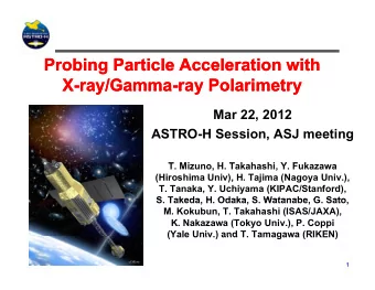
… the Belle II detector • The two innermost layers of the vertex detector will be consisted of DEPFET matrices • Ionizing Radiation from: • Beam-Gas Interaction • Synchrotron radiation will damage those matrices Ca. 1 Mrad/a (=10 kGy/a) • • Simulating of these various sources with x-ray radiation IMPRS Workshop 7/21/2009 3
What are DEPFETs? • Depend on sideward depletion: Internal Gate • Generated charges will be stored in the Internal Gate • Modulation of Drain- Source current • Clear operation necessary • Beneath Gate metallization: Layer of silicon dioxide Sensitive to ionizing radiation IMPRS Workshop 7/21/2009 4
Damage mechanism • Generataion of electron/hole pairs in the oxide • Mobility of holes is weak in comparison to electrons • Holes will be trapped near the interface and stay there for O(h) till O(a) • Also: Increase of interface state density IMPRS Workshop 7/21/2009 5
Dosimetry of the x-ray facility in Karlsruhe • To quantify the damage done by ionizing radiation Applied Dose is necessary • Calibration was given, Recheck it Problem Challenge started … IMPRS Workshop 7/21/2009 6
Recipe for succsesfull Calibration • X-ray source • Detector a) Fast readout, highly sensitive, good spectral response, low noise, superb amplifier b) If not (a), then find a compromise of (a) • Energy spectrum would be good a) Measure one b) Simulate one Thanks to my colleague: Oksana Brovchenko IMPRS Workshop 7/21/2009 7
1. Determine dose rate in silicon diode • Dose rate measurement via depleted diode • Measuring of reverse-current • X-ray photons generate electron/hole-pairs in Si- Bulk – Every charge carrier pair represents an energy of 3.6 eV – With the x-ray generated current one gets the deposited power, with the mass of the diode dose rate in Si IMPRS Workshop 7/21/2009 8
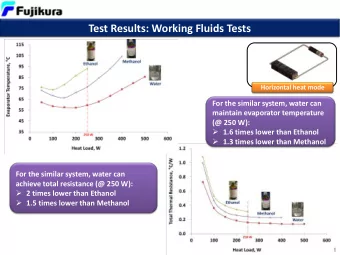
2. Making use of the spectrum • Spectrum of tungsten anode (including a 0.4 mm Be filtering, black) • Generate via absorption function of Zr a new transmitted spectrum (red) IMPRS Workshop 7/21/2009 9
3. Dose in SiO 2 • Dose measurement (diode) power of spectrum (Si, blue) is known • Original spectrum (black) Filter (Zr, red) Absorption in SiO 2 (green) • Final dose is determined IMPRS Workshop 7/21/2009 10
New dose rates New dose rates • Every dose rate matches to a specific set of parameters, let’s assume • U=60 kV (max. tube voltage) • I=33 mA (max. tube current) 1 • Distance is 155 mm ( ) D 2 r • Dose rate in silicon (300 µm) Gy | 0 , 305 D 60 , 33 , 155 , 300 Si kv mA mm µm s • Dose rate in silicon dioxide (180 nm) Gy | 0 , 239 D SiO 60 kV , 33 mA , 155 mm , 180 nm 2 s IMPRS Workshop 7/21/2009 7/21/2009 11 11
Back to the DEPFET: Setup and DAQ Study with a 6x16 Minimatrix • • Important contacts on PCB easy accessibility Drain contact needed probe • needle Several irradiation and • measurement steps Readout duration of input • characteristic of all 96 pixels ~ 6…7h • – min. 4 days of room temperature annealing DAQ via LabVIEW: Sweep of • Gate voltage, Drain current is measured IMPRS Workshop 7/21/2009 12
Results of input characteristics √I DS (U GS ) IMPRS Workshop 7/21/2009 13
Change of threshold voltage IMPRS Workshop 7/21/2009 14
Change of gain g m • Input characteristic curve fitted with – I=aU²+bU+c – Gain g m =mU+b via dI/dU m=2a no numeric deviation – Gain evaluated at Drain current = 50 µA • Maybe effect is part of setup and readout process needs to be rechecked to find out if effect still occurs IMPRS Workshop 7/21/2009 15
Outlook & Conclusions • Dosimetry – A good agreement between simulated spectrum and dose measurement with silicon diode has been found – Further investigations are under way: Spectrum has been measured (matches fine to the simulated one, except low energy photons • and L-Lines of tungsten) • Dosimetry with RadFETs have been done • DEPFET – Shift of threshold voltage matches to previous single pixel measurements (strongly dependent on gate voltage) – Spreading of threshold voltage after irradiation increased threshold voltage shift ∆ = ±0,12 V unirradiated • threshold voltage shift ∆ = ± 0,20 V at 142 krad (1.42 kGy) • threshold voltage shift ∆ = ±0,22 V at 2.37 Mrad (23.65 kGy) • – Impact on Belle II • Steering chips (Switcher) won‘t have problems with the spreading • Change of g m interferes on g q (via gate oxide capacitance). Variations in Drain-Source current may affect the current readout chip. IMPRS Workshop 7/21/2009 16
Backup Slides IMPRS Workshop 7/21/2009 17
Change of threshold voltage vs. Dose IMPRS Workshop 7/21/2009 18
Recommend
More recommend
Explore More Topics
Stay informed with curated content and fresh updates.
