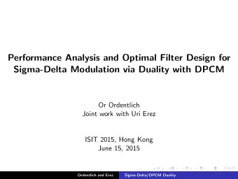
Delta-Sigma Time to Digital Converter Using Charge Pump and SAR ADC - PowerPoint PPT Presentation
Delta-Sigma Time to Digital Converter Using Charge Pump and SAR ADC IEICE General Conference 2015 Anugerah Firdauzi, Zule Xu, Masaya Miyahara, and Akira Matsuzawa Tokyo Institute of Technology Outline 2 Background Basic concept
Delta-Sigma Time to Digital Converter Using Charge Pump and SAR ADC IEICE General Conference 2015 Anugerah Firdauzi, Zule Xu, Masaya Miyahara, and Akira Matsuzawa Tokyo Institute of Technology
Outline 2 • Background • Basic concept • Circuit design • Simulation results • Conclusion 4/2/2015 Anugerah Firdauzi - Tokyo Tech
Background 3 • TDC Application Distance measurement Emitter – 3D camera L – Laser range finder – Time-of-flight (TOF) particle detector L Sensor – On chip jitter measurement 𝑴 = 𝒅. 𝒖/𝟑 – PLL and frequency synthesizer ADPLL • Contradictory requirements F ref Fv Digital TDC Filter – High resolution (~1ps) DCO – Wide input range (several ns) Counter 4/2/2015 Anugerah Firdauzi - Tokyo Tech
Previous Work 4 • Charge pump and SAR ADC • Time-to-charge conversion with SAR ADC high resolution • SAR-ADC: compact, sufficient range, and moderate speed • Challenge: high order SAR ADC is required 𝑢 𝑠𝑓𝑡 = 𝐷. 𝑊 𝑀𝑇𝐶 /𝐽 – High design complexity UP CK1 D out – Limited speed C V PFD … . – Large area DN CK2 SAR-ADC [Z.Xu , CICC ‘13] 4/2/2015 Anugerah Firdauzi - Tokyo Tech
Proposal: ΔΣ TDC 5 • Σ is realized by charging capacitor C and never reset it • Δ is realized by discharging/charging C through array of current source DAC at constant time for positive/negative output Σ E z -1 Δ Dout Σ Tin I CP - UP CK1 Δ D out C z -1 PFD DN CK2 I I I ... I CP t Logic + Q V t t - Current source DAC Q Δ =0.5Q 4/2/2015 Anugerah Firdauzi - Tokyo Tech
Timing Diagram 6 • 𝜠𝑾 𝒏𝒃𝒚 = ∆𝑾 𝑱𝑶,𝒏𝒃𝒚 + ∆𝑾 𝑬𝑩𝑫,𝒏𝒃𝒚 𝑱 𝑫𝑸 . 𝑼 𝑱𝑶,𝒏𝒃𝒚 𝟐 𝚻𝑱 𝑬𝑩𝑫 . 𝑼 𝑬𝑩𝑫 𝟑 𝑾 𝒔𝒇𝒈𝒒 − 𝑾 𝒔𝒇𝒈𝒐 = + • 𝑫 𝑬𝑩𝑫 𝑫 𝑬𝑩𝑫 CK1 ΔΣ thumb rule: CK2 ∆𝑾 𝑱𝑶,𝒏𝒃𝒚 = ∆𝑾 𝑬𝑩𝑫,𝒏𝒃𝒚 UP T IN T DAC DN V refp For VOP: Δ V IN - Δ V DAC VOP 1 Charging input VON SAR HIGH output discharge 2 conversion 1 2 1 3 V refn LOW output charge 3 Out (delay) 4/2/2015 Anugerah Firdauzi - Tokyo Tech
Multibit Quantizer Effect 7 For 𝑴 𝒖𝒊 order ΔΣ ADC with 𝑶 bit quantizer: • 𝟑 𝟑𝑴 + 𝟐 𝟑𝑴+𝟐 𝟒𝝆 𝟑 𝑶 − 𝟐 𝑷𝑻𝑺 𝑻𝑶𝑺 𝒆𝑪 = 𝟐𝟏 log • 𝟑 𝝆 𝑭𝑶𝑷𝑪 = (𝑻𝑶𝑺 𝒆𝑪 − 𝟐. 𝟖𝟕)/𝟕. 𝟏𝟑 • • Increasing quantizer size by one can improve ENOB 1-1.5 bit 30 [L,N] [5,4] [4,4] [3,4] 25 • Target: [2,4] [1,7] – 1 st order ΔΣ TDC 20 ↓ ENOB [1,1] – Quantizer 4 bit 15 – OSR = 100 10 – ENOB = 13 bit Target 5 0 4/2/2015 Anugerah Firdauzi - Tokyo Tech 1 10 100 1000 OSR
Simulation Result 8 0 • Ideal model using MATLAB SNDR = 72.42 dB 1ns input -20 ENOB = 11.74 bit • 4 bit quantizer SNDR = 73.63 dB ENOB = 11.94 bit -40 • Input = ± 1ns at 52kHz -60 PSD [dB] • BW = 1MHz -80 • OSR = 100 -100 1ps noise -120 ideal • Result: -140 20dB/dec BW ENOB > 11bit -160 4 5 6 7 8 10 10 10 10 10 Effective resolution < 0.9ps Frequency [Hz] 4/2/2015 Anugerah Firdauzi - Tokyo Tech
Conclusion 9 • A new approach for TDC by using ΔΣ architecture is proposed. • ΔΣ TDC implemented by using CP SAR ADC, and current source DAC gives first order noise shaping and high resolution for moderate bandwidth while keeping the input range large and power consumption low 4/2/2015 Anugerah Firdauzi - Tokyo Tech
Recommend
More recommend
Explore More Topics
Stay informed with curated content and fresh updates.
