Computer Architecture Foundations of Global Networked Computing: - PowerPoint PPT Presentation
IWKS 3300: NAND to Tetris Spring 2019 John K. Bennett Computer Architecture Foundations of Global Networked Computing: Building a Modern Computer From First Principles This course is based upon the work of Noam Nisan and Shimon Schocken. More
IWKS 3300: NAND to Tetris Spring 2019 John K. Bennett Computer Architecture Foundations of Global Networked Computing: Building a Modern Computer From First Principles This course is based upon the work of Noam Nisan and Shimon Schocken. More information can be found at (www.nand2tetris.org).
A Brief History of Computer Architecture
Abacus (2700 – 2300 BC; Sumeria) Sexagesimal (base-60) number system
Blaise Pascal (1623-62)
Jacquard Loom (1801)
AVL Jacquard Loom (2016)
Atanasoff – Berry Computer (1937-42; vacuum tubes)
Zuse Z3 (1941-43; relays)
Eniac (1943-46; vacuum tubes)
Eniac
Eniac
Eniac
Illiac I / OrdVac (1951) Ordnance Discrete Variable Automatic Computer
R1- Rice Research Computer (1959)
IBM 360 (1964)
R2- Rice Research Computer (1973)
Hexadecimal Calculator
Cray 1 (1975)
Cray 1 (1975)
Cray 2 (1985)
The Xerox Alto, 1973 First personal workstation; first wide deployment of: Bit-map graphics Mouse WYSIWYG editing Hosted the invention of: Local-area networking Laser printing All of modern client / server distributed computing
MITS Altair 8800 (1975)
Basic on an 8-bit Computer
Apple I (1975-6)
Apple II (1977)
TRS 80 (1977)
Apple Lisa (1979)
IBM PC (1981)
UW Eden Node Machine (1982)
IBM PC XT (1983)
Apple Macintosh (1984)
Sun 1-3 Workstations (1982-85)
iPhone (2007)
Amazon Kindle (2007)
iPad (2009)
Von Neumann Machine (circa 1940) CPU Input device Arithmetic Logic Memory Unit (ALU) (data Registers + instructions) Output device Control Gordon Moore, Andy Grove (and others) John Von Neumann (and others) ... made it possible ... made it small and fast.
Harvard Mark 1 (circa 1940) Howard Aiken
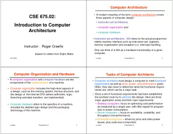
Processing logic: fetch-execute cycle CPU Input device Arithmetic Logic Memory Unit (ALU) (data Registers + instructions) Output device Control Executing the current instruction involves one or more of the following tasks: Have the ALU compute some function out = f (register values) Write the ALU output to selected registers As a side-effect of this computation, determine what instruction to fetch and execute next.
The Hack chip-set and hardware platform Computer Architecture Combinatorial Chips Sequential Chips Elementary Gates Memory HalfAdder DFF Nand CPU FullAdder Bit Not done Computer Add16 Register And Inc16 RAM8 Or this lecture ALU RAM64 Xor RAM512 Mux done RAM4K Dmux RAM16K Not16 PC And16 Or16 done Mux16 Or8Way Mux4Way16 Mux8Way16 DMux4Way DMux8Way
The Hack Computer A 16-bit Harvard platform (data and instructions are separate) The instruction memory and the data memory are physically separate Screen: 512 rows by 256 columns, black and white Keyboard: standard (memory-mapped to a specific RAM address) Designed to execute programs written in the Hack machine language Can be easily built from the chip-set that we have built so far in the course Main parts of the Hack computer: Instruction memory (ROM) Memory (RAM): • Data memory • Screen (memory map) • Keyboard (memory map) CPU Computer (the framework that holds everything together).
Where We Are Headed inM writeM Instruction Data outM instruction Memory CPU Memory addressM (ROM32K) (Memory) pc reset CHIP Computer { IN reset; PARTS: // implementation missing }
Instruction Memory out address ROM32K 16 15 Function: The ROM is pre-loaded with a program written in the Hack machine language The ROM chip always emits a 16-bit number: out = ROM32K[address] This number is interpreted as the current instruction . ROM[2 n ] is implemented using 8 ROM[2 n-3 ]’s, an 8:1 multiplexor, and a 1:8 demultiplexor.
Data Memory load in out RAM16K 16 16 address 15 Function: When read, the RAM16K chip always emits a 16-bit value: out = RAM16K[address] A 16 bit value is required to write to the RAM16K chip: RAM16K[address] = in & load & clock RAM[2 n ] is implemented using 4 or 8 RAM[2 n-3 ] ’ s, an 8:1 multiplexor, and a 1:8 demultiplexor.
Data Memory load Low-level (hardware) read/write logic: To read RAM[ k ] : set address to k, probe out in out To write RAM[ k ] =x: set address to k, RAM16K set in to x, 16 16 set load to 1, address run the clock 15 High-level (OS) read/write logic: To read RAM[ k ] : use the OS command out = peek( k ) To write RAM[ k ] =x: use the OS command poke( k , x ) peek and poke are OS commands whose implementation should effect the same behavior as the low-level commands More about peek and poke this later in the course, when we write the OS.
Screen The bit contents of the Screen load chip are called the “screen memory map” in out Simulated screen: 16 Screen 16 address 15 Physical Screen The simulated The Screen chip emulates basic RAM chip functionality: 256 by 512 B&W screen read logic: out = Screen[address] When loaded into the write logic: if load then Screen[address] = in hardware simulator, the built-in Screen.hdl chip Side effect: opens up a screen window; the simulator then Continuously refreshes a 256 by 512 black-and-white refreshes this window from screen device the screen memory map several times each second.
Screen Memory Map 16384 (0x4000) 0 0011000000000000 0 1 2 3 4 5 6 7 . . . 511 1 0000000000000000 0 . . . In the Hack platform, the row 0 . 1 . . . . . screen is implemented 31 0000000000000000 as an 8K 16-bit RAM . . 32 0001110000000000 . . 33 0000000000000000 chip. . . . row 1 . . 63 0000000000000000 255 . . . Screen 8129 0100100000000000 8130 0000000000000000 row . . 255 . refresh several times each second 8160 0000000000000000 How to set the (row,col) pixel of the screen to black or to white: Low-level (machine language): Set the col%16 bit of the word found at Screen[row*32+col/16] to 1 or to 0 ( col/16 is integer division) High-level: Use the OS command drawPixel(row,col) (effects the same operation, discussed later in the course, when we write the OS).
Keyboard Simulated keyboard: out Keyboard 16 Keyboard Keyboard chip: a single memory-mapped 16-bit register Input: scan-code (16-bit value) of the currently The simulated pressed key, or 0 if no key is pressed keyboard enabler button Output: same Special keys: The keyboard is implemented as a built-in Keyboard.hdl chip. When this java chip is loaded into the simulator, it connects to the regular keyboard and pipes the scan-code of the currently pressed key to the keyboard memory map. How to read the keyboard: Low-level (hardware): probe the contents of the Keyboard chip at RAM location: 24576 (0x6000) High-level: use the OS command keyPressed() (effects the same operation, discussed later in the course, when we write the OS).
Memory Physical Implementation load The Memory chip is essentially a package Memory that integrates the three chip-parts RAM16K, Screen, and Keyboard into a 0 single, contiguous address space. in This packaging effects the programmer’s RAM16K view of the memory, as well as the 16 out (16K mem. chip) necessary I/O side-effects. 16 16383 16384 Screen address (8K mem. chip) 15 24575 Screen Keyboard 24576 (one register) Keyboard Access logic: Access to any address from 0 to 16,383 results in accessing the RAM16K chip-part Access to any address from 16,384 to 24,575 results in accessing the Screen chip-part Access to address 24,576 results in accessing the keyboard chip-part Access to any other address is invalid.
Memory: Programmer’s View Memory Data Screen memory map Screen Keyboard map Keyboard Using the memory: To record or recall values (e.g. variables, objects, arrays), use the first 16K words of the memory: (0x0000-3FFF) To write to the screen (or read the screen), use the next 8K words of the memory: (0x4000-5FFF) To read which key is currently pressed, use the next word of the memory: (0x6000).
LogicCircuit Keyboard Configuration How to read the keyboard: Low-level (hardware): probe the contents of the Keyboard chip at RAM location: 24576 (0x6000) High-level: use the OS command keyPressed() (effects the same operation, discussed later in the course, when we write the OS).
LogicCircuit Configuration for the Hack Screen The Screen chip emulates basic RAM chip functionality: read logic: out = Screen[address] write logic: if load then Screen[address] = in Side effect: Continuously refreshes a 256 by 512 black-and-white screen device
LogicCircuit Configuration of the Hack Instruction Memory Access logic: Access to any address from 0 to 16,383 results in accessing the RAM16K chip-part Access to any address from 16,384 to 24,575 results in accessing the Screen chip-part Access to address 24,576 results in accessing the keyboard chip-part Access to any other address is invalid.
Recommend
More recommend
Explore More Topics
Stay informed with curated content and fresh updates.






![Mostly Core Constructing real world sites [mostly] using Drupal 8 core Karen Stevenson](https://c.sambuz.com/910537/mostly-core-s.webp)