Chapter 4 The Wire Wiring analysis is essential for: Speed Power - PowerPoint PPT Presentation
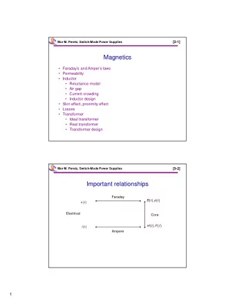
Digital IC-Design The Wire & decreasing feature sizes Dynamic behavior change in deep submicron A Active elements are less dominant i l l d i Chapter 4 The Wire Wiring analysis is essential for: Speed Power Reliability Parasitics
Digital IC-Design The Wire & decreasing feature sizes Dynamic behavior change in deep submicron A Active elements are less dominant i l l d i Chapter 4 The Wire Wiring analysis is essential for: Speed Power Reliability Parasitics Wire Parasitics Bonding wire Wire parasitics Wire Parasitic classes inductance Capacitive Resistive Wire Inductive Substrate Reduces Performance Increase Power Consumption Affect Reliability Pin capacitance 1
Supply is Provided from Outside Resistive (Inductive) Parasitics V DD DD Package Package Capacitance (pF) Capacitance (pF) Inductance (nH) Inductance (nH) R Wire R V DD 68 Pin Plastic DIP 4 35 68 Pin Ceramic DIP 7 20 I Switch 256 Pin Grid Array 5 15 V Bond Wire 1 1 Solder Bump Solder Bump 0 5 0.5 0.1 0 1 Source: Sze Interconnect Capacitive and Inductive Coupling Connection Probability V A voltage or a current 0.08 change may influence change may influence C Coupling Local Wires V the signal on a parallel 0.06 wire, especially on: Global Wires 0.04 Long wires Sub micron technologies I M t Mutual l Several metal layers S l t l l Gl b l Wi Global Wires do not d t 0.02 scale with the Inductance technology I 0.2 0.4 0.6 0.8 1.0 Wire Length/Chip Diagonal Length 2
Metal Layers Metal Layers - Not a 2D problem!!! Transistors Transistors Long wires affect Long wires affect Tungsten Contacts Tungsten Contacts the performance the performance Capacitance: Fringing Capacitance: Parallel Plate H W SiO 2 SiO L ε WL W = C ox H Metal/Poly etc. t ox W W H H t ox t Substrate ε = × − 15 Permitivity 3.5 10 F / cm for SiO ox 2 3
Metal Layers Capacitance Values Contacts (via) Metal Typical 0.35 μ process μ p yp Plate Cap. fF/um 2 Fringing Cap. fF/um Layer Poly to Substrate 0,119 0,051 Metal1 to Substrate 0,031 0,043 Metal2 to Substrate 0,012 0,031 Note the Size! Per fringe! Fringing C Example: Calculate the Wire Cap. Impact of Fringing Capacitance 0.35 μ Technology Capacitance pF/cm 10x10 mm Chip 6 Fringing capacitance 0 031 10 − ⋅ 15 0.031 10 = × ⋅ − × = C 6 6 0.1 1 10 dominates for plate − 12 10 T/H=1 small W/H = 3.1 pF 1 T/H=0.5 In 0.35 μ ⋅ − 15 0.043 10 = × × = C 2 0.1 W W ≈ H ≈ T fringe − 6 10 C plate = plate 8.6 8 6 pF pF T CLK = + = C C C 0.1 0.1 11.7 pF tot plate fringe 0.4 1 4 10 H W/H Total Length 0.1 m Δ L = 15mm 1 μ m wide 4
Interwire Capacitance Interwire Capacitance Metal2 Typical 0.35 μ process Area Cap. fF/um 2 Fringing Cap. fF/um Layer Cross-talk Metal1 Poly to Metal1 0,054 0,050 Metal1 to Metal2 0,035 0,043 Poly to Metal2 0,015 0,033 Poly Poly Per fringe! Substrate Wire Resistance Sheet Resistance Sheet Resistance Typical Values 0.25 μ m technology ρ L L = × = × R R R R W H W Material M i l Sheet Resistance Sh R i R 50-150 Ω / � Diffusion 1000-15000 Ω / � Well R R 150-200 Ω / � Polysilicon R L R R R 4-5 Ω / � Poly with Silicide R W 0.05-0.10 Ω / � R R Aluminum R H R Metal/Poly etc. 5
Example: Calculate the Wire Resistance Silicide 0.25 μ Technology 10x10 mm Chip Silicide to reduce the poly resistance Conductivity: Silicide L 8-10 times better 0.01 Polysilicon = × = × = R R � 0.1 than Poly ⋅ − W 6 SiO 2 1 10 n + n + p - = Ω 1 k CLK Advanced technologies have silicide on polysilicon Longest Length = 10mm Δ L = 15mm 1 μ m wide Silicides: WSi 2 , TiSi 2 , PtSi 2 , and TaSi Optimal wiresizing Optimized tree Minimum delay wire has an exponential taper Optimal tapering improves delay by about 8% Source Sink 1 Implemented with boxes Sink 2 Source: Wayne Wolf 6
The Lumped Model Delay Definitions V out t − V IN = − V e RC V (1 ) out out in in Driver C wire = − 50% t t t r 90 10 t pHL t pLH t R driver t − V OUT 90% = − V V e V V V out V RC RC (1 (1 ) ) out in 50% C lumped Model 10% t f t r t Rise-Fall time Distributed RC-Line t − = − = − V e RC V t t t (1 ) ; out in r 90 10 R R R V out t − 10 Lumped Lumped = − ⇔ C V e V RC C 0.1 (1 ) C in in Model t − 10 = ⇔ e RC 0.9 r Δ L = − t RC r Δ L r Δ L ln(0.9) 10 = − t RC ln(0.1) Distributed c Δ L c Δ L c Δ L c Δ L c Δ L c Δ L 90 Model = − = − + = = t t t RC t RC ( ln(0.1) ln(0.9)) 2.2 r 90 10 r L = − = = t RC t RC ln(0.5) 0.69 50 50 7
Driving a Wire RC-Models R s R w V out V out Lum ped Distributed C w t p (0 -> 50% ) 0.69 RC 0.38 RC RC (0 -> 63% ) RC 0.5 RC t r (10% -> 90% ) 2.2 RC 0.9 RC = + = + t R C R C R R C 2.2 0.9 (2.2 0.9 ) Lumped model tends to be pessimistic r s w w w s w w RC-Models The Elmore Delay R R R 2 2 = + + + + + + + + + τ R C (R R )C (R R R )C (R R R R )C � C C 1 1 1 2 2 1 2 3 3 1 2 3 4 4 C 2 2 R 1 R 2 R 3 R 4 R 5 R 6 R R R R R 2 2 4 2 4 C C C C C C 1 C 2 C 3 C 4 C 5 C 6 4 2 4 2 2 R R R R R R R 3 3 3 3 3 3 6 6 3 3 3 3 6 6 C C C C C C C 6 3 3 6 3 3 3 π -Models T-Models 8
Electro Migration ≈ The Elmore Delay I 1mA/um DC, max = + + + + + + τ R C (R R )C (R R R )C R C 1 1 1 2 2 1 2 3 3 1 4 C 4 is loaded through R 1 R 4 C 4 R 4 do not affect the R 1 delay at V out V in C 1 C R 3 R 2 V out C 2 C 3 Electro Migration Avoiding Electro Migration Many contacts for higher currents 9
Recommend
More recommend
Explore More Topics
Stay informed with curated content and fresh updates.


