CE B02: 402.4 Endcap Calorimeter: Planning for CD-3a Harry Cheung - PowerPoint PPT Presentation
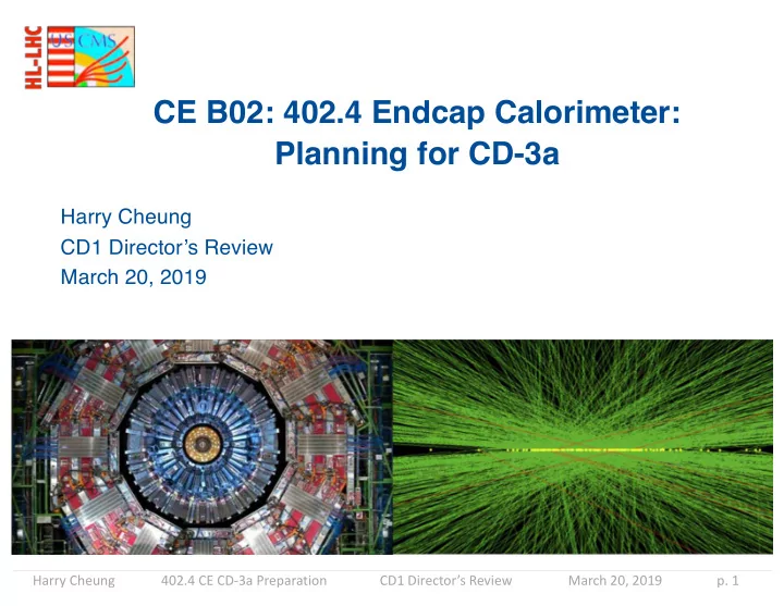
CE B02: 402.4 Endcap Calorimeter: Planning for CD-3a Harry Cheung CD1 Directors Review March 20, 2019 Harry Cheung 402.4 CE CD-3a Preparation CD1 Directors Review March 20, 2019 p. 1 Outline Introduction:
CE B02: 402.4 Endcap Calorimeter: Planning for CD-3a Harry Cheung CD1 Director’s Review March 20, 2019 Harry Cheung 402.4 CE CD-3a Preparation CD1 Director’s Review March 20, 2019 p. 1
Outline § Introduction: Silicon Sensors § CD-3a scope; Sensor Scope and Deliverables § Sensor Design § Technical Progress with Updates since Jun 2018 IPR § Path to 8” wafer sensor qualification § R&D Needed Before Production § Schedule § Risks § Resource Optimization § ES&H, QA and QC § Cost § Response to June 2018 IPR § Progress towards CD-3a § Summary Harry Cheung 402.4 CE CD-3a Preparation CD1 Director’s Review March 20, 2019 p. 2
Scope for CD-3a § Scope Planned for CD-3a § Preproduction and production silicon sensors § QC of these silicon sensors § Sensors are a long lead item as the production takes time § Need to proceed with a single vendor who has finite production capacity § Sensors are a critical component needed to start module production § Significant QC effort, important to get started early § Sensor design is close to final, and almost completely validated § Will be ready for a CD-3a Harry Cheung 402.4 CE CD-3a Preparation CD1 Director’s Review March 20, 2019 p. 3
Scope - Sensors § The US will purchase standard and odd-sized silicon sensors for the endcap calorimeter: the US commitment is fixed to 7290 standard (76%) and 1812 odd-sized sensors (100%) for the hadronic section (CE-H) § Quote from vendor specifies payment only for sensors which meet quality criteria on IV/CV, therefore the effective wafer yield is expected to be very high § The US is responsible for design, specification, and testing (including radiation qualification) of the silicon sensors in collaboration with the international CMS § The US has responsibility to carry out associated TCAD simulations Main Sensor (Overall) ・N+ in p chip size : 183474±40 active area: 181677 ・198 channels 8 1 ・P-stop isolation 14 13 Calibration Cells chip size : 166570±40 active area: 164774 10465 Unit [μm] 10465 190 198 12084 12084 CONFIDENTIAL 3 Harry Cheung 402.4 CE CD-3a Preparation CD1 Director’s Review March 20, 2019 p. 4
Design Considerations for Sensors Charge #2 § The sensors must be sufficiently radiation hard to allow operation through the lifetime of HL-LHC, radiation tolerant to ~10 16 n eq /cm 2 at inner radius § Reconstruction of MIP and radiation hardness (EC-sci-engr-002 and EC-engr-021) § Sensor design must be compatible with § High transverse and longitudinal granularity and cell size (EC-sci-engr-004, EC-engr-022) § Good energy resolution for EM, jet and Etmiss (EC-sci-engr-006)) § Good pile-up mitigation (EC-sci-engr-007) § Precision timing of showers and time resolution (EC-sci-engr-009, EC-engr-023) § Minimal dead area (EC-engr-025) § Robust design of internal and peripheral structures § Reliability and maintainability (EC-sci-engr-010) § Large area hexagonal sensors, low cost per sensor, efficient tiling § EC sensors from 8-inch wafers (EC-engr-024) § Low temperature (-30 o C) operation § Production sensor quality must be monitored to insure that good channel, depletion voltage, and leakage current specifications are met § All vendors and sensor types must be fully qualified for radiation hardness Harry Cheung 402.4 CE CD-3a Preparation CD1 Director’s Review March 20, 2019 p. 5
Sensor Design - I Charge #2 Standard Standard Odd-size Odd-sized 192 Large cells 432 Small cells Chop2 sensor Half sensor § Sensor design is practically done. Fundamental parameters (pad shapes, gaps, biasing, guard ring, and implants) are well- understood. Operational experience with 6-inch sensors is excellent. Starting to finalize 8” production specs with vendor. § Two classes of 8-inch modules: standard and odd-sized § Standard silicon sensors come either with large 1.18 cm 2 or small 0.52 cm 2 cells with three different active thicknesses: 120, 200 and 300 µ m Harry Cheung 402.4 CE CD-3a Preparation CD1 Director’s Review March 20, 2019 p. 6
Sensor Design - II Charge #2 Sensor Tiling for Layer 32 Active Thick. 120 200 300 Chop2 Sensors ( µ m) Cell size (cm 2 ) 0.52 1.18 1.18 120 µ m Sensors Cell cap. (pf) 50 65 45 Exp. fluence 0.2-1 × 10 16 0.5-2.5 × 10 15 1-5 × 10 14 (n eq /cm 2 ) Largest dose 100 20 3 (MRad) R in , R out (cm) ~35 : ~75 ~70 : ~100 ~100 : ~180 200 µ m Sensors S/N MIP (initial) 4.5 6 11 300 µ m Sensors S/N MIP (3,000 2.2 2.3 4.7 fb -1 ) Standard Sensors Half Sensors § Silicon sensor parameters are optimized such that good signal-to-noise ( S/N ) ratio for MIPs is maintained throughout the life of the detector (3,000 fb -1 ) at HL-LHC § Design of CE-H layers is optimized by geographically placing appropriate type of sensors transversally Harry Cheung 402.4 CE CD-3a Preparation CD1 Director’s Review March 20, 2019 p. 7
Sensor Design - III Charge #2 The high radiation drives sensor choices § Thin active layer sensors have + Lower total leakage current + Higher fields, better charge collection per unit thickness + Lower depletion voltage - More difficult to fabricate § Sensors on 8” (200 mm) wafers § 3 different active layer thicknesses § 300 micron active thickness, FZ p-type with 300 micron physical thickness § 200 micron active thickness, FZ p-type with 200 micron physical thickness § 120 micron active thickness, epitaxial p-type with 300 micron physical thickness Need to operate at low temperature to control leakage current and depletion voltage (-30 ℃ ) Harry Cheung 402.4 CE CD-3a Preparation CD1 Director’s Review March 20, 2019 p. 8
Sensor Design - IV Charge #2 § Layout partially driven by trigger cells Main Sensor (Overall) § Four cell trigger clusters ・N+ in p chip size : 183474±40 active area: 181677 ・198 channels 8 1 § Sensors are optimized for assembly and testing 14 ・P-stop isolation 13 § Large pads Calibration Cells chip size : 166570±40 active area: 164774 § Laser test holes in metal 10465 Unit [μm] 10465 § Calibration pads 190 198 12084 12084 § Minimize gap between module active areas – thin guard rings CONFIDENTIAL 3 § Initial designs used in the test beam campaigns were finalized for 8” sensors partially based on US design concepts § Studied inter-pad gaps and guard ring designs § TCAD: capacitance, leakage current, jumper designs and radiation effects Wirebond pads Hole for laser calibration Pad number Harry Cheung 402.4 CE CD-3a Preparation CD1 Director’s Review March 20, 2019 p. 9
R&D Achieved so far - I Charge #2 § The S/N performance goals are achieved: silicon sensors and module components function as expected § Beam tests at Fermilab (2016) and CERN (2016-18) have been performed using fully functional 6-inch sensors with electrons and hadrons § 16 modules with SKIROC in 2016 and 20 (94) modules with SKIROC2-CMS in 2017 (2018) have been tested 2016 2016 2017 2018 Harry Cheung 402.4 CE CD-3a Preparation CD1 Director’s Review March 20, 2019 p. 10
R&D Achieved so far - II Charge #2 § Leakage current (LC) density increases § The test structures prove with neutron fluence: expected, extremely useful in irradiation simulated and CV/IV measurements are in good agreement. D I = a V F studies and consequently in where at room temperature a = 4.0x10 - tuning many TCAD parameters 17 A/cm § Irradiation studies are ramping § LC extracted fluence and activation foil up for 8” wafer sensors measurements are in good agreement (~x2 at highest fluences) in irradiation studies performed at RINSC with test structures Harry Cheung 402.4 CE CD-3a Preparation CD1 Director’s Review March 20, 2019 p. 11
Path to 8” Sensor Qualification Charge #2 2017: First Prototype 8” HPK sensors, produced with stepper • Received 300 µm FZ (12), 200 µm FZ (12), & 120 µm epi (6) • Indicative of excellent underlying quality • Tooling issue (back-side scratches) identified & corrected 2018: Prototype 8” HPK sensors with full-wafer mask aligner • Received 14 x 300 µm FZ, 14 x 200µm FZ in November 2018 • Excellent underlying quality, but not yet perfect • Tooling issue (front-side scratches) identified & corrected • Back-side handling issue (increase LC in few cells) • Received 12 x 120 µm epi in February 2019 • Delayed by epi wafer procurement, then held until production of 300um/200um sensors understood and issues addressed Example 1: sensor with scratch around pads #86-87 Example 2: an excellent, defect free, sensor Example 3: sensor with scratch around pads #86-87, and a few other defective pads HPK HPK HPK Harry Cheung 402.4 CE CD-3a Preparation CD1 Director’s Review March 20, 2019 p. 12
Full Lithography Sensor Tests Charge #2 § CV and IV Measurements of 200 μm & 300 μm sensors § Results as expected, understanding variations across wafer § Some issues with scratches (HPK handling), and handling during testing; planned modifications to address these § Good comparison between HPK and CERN measurements, need to understand differences in detail for mass production. Depletion Voltage Leakage Current Harry Cheung 402.4 CE CD-3a Preparation CD1 Director’s Review March 20, 2019 p. 13
Recommend
More recommend
Explore More Topics
Stay informed with curated content and fresh updates.
