A GUIDE TO CRYOGENIC APPLICATIONS OF SIPMS Relatively young field - PowerPoint PPT Presentation
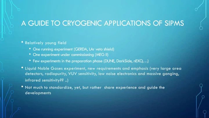
A GUIDE TO CRYOGENIC APPLICATIONS OF SIPMS Relatively young field One running experiment (GERDA, LAr veto shield) One experiment under commissioning (MEG II) Few experiments in the preparation phase (DUNE, DarkSide, nEXO,)
A GUIDE TO CRYOGENIC APPLICATIONS OF SIPMS • Relatively young field • One running experiment (GERDA, LAr veto shield) • One experiment under commissioning (MEG II) • Few experiments in the preparation phase (DUNE, DarkSide, nEXO,…) • Liquid Noble Gases experiment, new requirements and emphasis (very large area detectors, radiopurity, VUV sensitivity, low noise electronics and massive ganging, infrared sensitivity?? ..) • Not much to standardize, yet, but rather share experience and guide the developments
MENU • Review of the existing/planned experiments (Fabrice Retiere) • Physics of SiPMs at cryogenic temperatures (Gianmaria Collazuol) • Review of the readout electronics approaches (Wataru Ootani) • Testing setups at cryogenic temperatures (Andrii Nagai) • Reliability issues for large scale applications (Vishnu Zutshi) • Interesting new contributions
PHYSICS OF SIPMS AT CRYOGENIC TEMPERATURES AND IMPLICATIONS FOR THEIR PERFORMANCE AND CHARACTERISTICS G.Collazuol, Department of Physics and AstronomyUnversita` di Padova and INFN A.Para, Fermilab ICASiPM 2018, Schwetzingen
SUMMARY • Cryogenic experiments (LXe/LAR) use SiPMs in the regime where the fundamental physics of silicon changes considerably (source of the figures: Gutierrez, Dean, Claeys “Low Temperature Electronics: Physics, Devices, Circuits and Applications”) • (Some) SiPMs characteristics may vary significantly from room temperature to the operating conditions • Cold/warm temperature variation may depend on the specific device design (room for the device optimization)
FREE CARRIERS IN DOPED SILICON LXe LAr Room temperature Donors/acceptors fully ionized by thermal excitations . Silicon is a semiconductor. Free carriers produced by a temperature- dependent combination of • Thermal excitations • ‘field-assisted’ excitations • tunneling Donors/acceptors levels filled up. Insulator.
SILICON PROPERTIES AT LOW T: HIGHER CARRIER MOBILITY • Carrier mobility è avalanche development, time development • Temperature variation depends on doping profiles and electric fields è effect onSiPM performance may depend on the details of the SiPM design 6
SILICON PROPERTIES AT LOW T: IONIZATION COEFFICIENTS • Impact ionization coefficient è avalanche development, time development, breakdown voltage • Electron/hole variation è Wavelength dependence of PDE • Temperature variation depends on doping profiles and electric fields è effect onSiPM performance may depend on the detais of the SiPM design 7
AVALANCHE BREAKDOWN: TEMPERATURE VARIATION Avalanche breakdown V is expected to show a non linear dependence on T (depending of the junction type and doping concentration) Breakdown V decreasing with T due to increasing mobility NOTE: in freeze-out regime Zener (tunnel) breakdown could be relevant. → negative Temperature coefficient (increasing with decreasing T) Crowell and Sze More recent model by Crowell and Okuto after Shockley, Wolff, Baraff, Sze and Ridley. 8
SILICON ABSORPTION LENGTH AT LOW TEMPERATURES • Variation of the wavelength-dependence of PDE with temperature 9 A.PARA - G.COLLAZUOL - CRYOGENIC BEHAVIOUR OF SILICON PMS
IN ADDITION: QUENCHING RESISTOR Adopting metal quenching resistor Improved temperature stability 10 A.PARA - G.COLLAZUOL - CRYOGENIC BEHAVIOUR OF SILICON PMS
PULSE SHAPE: DEPENDENCE ON TEMPERATURE The two current components behave differently with Temperature → fast component is independent of T because C tot couples to external R load → slow component is dependent on T because C d,q couple to R q (T) H.Otono, et al. PD07 HPK MPPC high pass filter / shaping → recover fast signals HPK MPPC Akiba et al Optics Express 17 (2009) 16885 11 A.PARA - G.COLLAZUOL - CRYOGENIC BEHAVIOUR OF SILICON PMS
REVERSE BIAS I-V CURVES → DARK CURRENT AND V BD Dark current decreases rapidly with T Reverse I-V characteristics at fixed T at rate ~ x2 / 10K Breakdown Voltage vs T FBK devices Breakdown voltage decreases at low T due to larger carriers mobility → larger ionization rate (electric E field fixed) G.C. et al NIM A628 (2011) 389 12
V BD VS T → TEMPERAURE COEFFICIENT ( D V STABILITY) Breakdown Voltage Vbr measured by fitting single ~80 mV/K p.e. charge vs bias voltage Temperature coefficient (pulsed mode) (above 240K) D v br /V br / D T ~0.25 %/K the line is for Improved FBK device eye guide dV br /dT (V/K) stability at low T G.C. et al NIM A628 (2011) 389 D v br /V br / D T ~0.20 %/K HPK device (400 pixels) T (K) J.Csathy et al NIM A 654 (2011) 225 13
PULSE SHAPE VS T Alberto Gola – IEEE NSS-MIC 2015 A.Para - G.Collazuol - Cryogenic behaviour of 14 Silicon PMs
sources of DCR contribution to DCR DARK CURRENT VS T from diffusion of minority carriers negligible below 350K Noise mainly comes from the high E Field region (no 1) Generation/Recombination SRH whole depletion region) noise (enhanced by trap assisted tunneling) FBK devices I re ve rse ~ T 1.5 exp − E a ct K B T Conventional constant D V SRH positive T coefficient trap assisted tunneling x1000 2) Band-to-band Tunneling noise (strong dependence on the Electric field profile) x10 negative T coefficient x10 x1000 E field engineering is Tunneling noise dominating for T<200K crucial for min. DCR (sharp high E field region → higher noise) (esp. at low T) 15 A.PARA - G.COLLAZUOL - CRYOGENIC BEHAVIOUR OF SILICON PMS
DARK COUNT RATE VS TEMPERATURE (CONSTANT D V) Measurement of counting rate of ≥ 1p.e. D V = 1.5V at fixed D V=1.5V d (→ constant gain) e c n a h n e d l e i f H R DCR~ T 1.5 exp − E a ct S K B T Activation energy E act ~0.36eV Tunneling ??? onset of carriers freeze-out (carrier losses at very low T due to ionized impurities acting as shallow traps) Under investigation 16
OPTIMIZE SIPM FOR CRYOGENIC OPERATION: FBK Alberto Gola – IEEE NSS-MIC 2015 17
AFTER-PULSES VS T (CONSTANT DV) Measurement by waveform analysis: - trigger on single carrier pulses (with no preceding pulses D V = 1.5V within D t=5 µ s), count subsequent pulses within D t=5 µ s (find the after-pulsing rate r AP ) FBK devices - Subtract dark count contribution - extract after-pulsing probability P AP corrected for after-pulsing cascade r AP P AP = 1+ r AP After-pulses envelope • Few % at room T • ~constant down to ~120K AP “trains” G.C. et al NIM A628 (2011) 389 T decreasing: increase of characteristic time constants of traps ( t traps ) compensated by increasing cell recovery time (R q ) • several % below 100K The growth of micro-cell recharge time T<100K: additional trapping centers activated help reducing the after-pulsing at low T possibly related to onset of carriers freeze-out 18 A.PARA - G.COLLAZUOL - CRYOGENIC BEHAVIOUR OF SILICON PMS
QUICK GUIDE: DARK RATE, AFTERPULSES, CROSS TALK After-Pulsing swift Dark Noise Rate increase below 100K dumped at low T P AP ~ independent of T above 100K !!! SRH vs Tunneling different slope d DR/ dD V (cfr PDE vs D V) (slight reduction expected due to lower PDE for large l at low T) Gain and Cross-Talk are independent of T 19 A.PARA - G.COLLAZUOL - CRYOGENIC BEHAVIOUR OF SILICON PMS
SPECTRAL SENSITIVITY PDE vs l ( D V constant) PDE D V vs ( l constant) PDE Simulation Data G.C. et al NIM A628 (2011) 389 l =400nm T=50,150,...,300K saturation starts earlier at low T D V (V) PDE spectrum at low T peaks at shorter l Data D V = 2V T=300K T=250K T=150K Simulation T=50K l ( µ m) 20
TIMING AT LOW TEMPERATURE • Timing resolution improves with decreasing T • Lower jitter at low T due to higher mobility: a) avalanche process is faster b) reduced fluctuations NOTE: • Ultimate timing resolution not likely to be a major factor for LXe/LAr experiments single photon FBK timing resolution devices G.C. (2011, unpublished) 21 A.PARA - G.COLLAZUOL - CRYOGENIC BEHAVIOUR OF SILICON PMS
SUMMARY • Area of intensive research. Large body of results (very selected examples shown for the illustration) confirming the ‘standard model’ of SiPMs (no physics beyond the standard model, yet) • Useful guide for the developments of specialized SIPMs (large area/low noise, VUV,..) • Useful guide for development of testing and characterization techniques and strategies. For example: different physics processes dominate at different temperatures hence some of the characteristics measured at cryogenic temperatures may not be well correlated with the same characteristics measured at room temperatures è need for dedicated cryogenic testing setups.
Recommend
More recommend
Explore More Topics
Stay informed with curated content and fresh updates.
