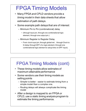
VARIUS: A Model of Process Variation and Resulting Timing Errors for - PowerPoint PPT Presentation
VARIUS: A Model of Process Variation and Resulting Timing Errors for Microarchitects Smruti R. Sarangi, Brian Greskamp, Radu Teodorescu, J Jun Nakano, Abhishek Tiwari and Josep Torrellas N k Abhi h k Ti i d J T ll University of Illinois
VARIUS: A Model of Process Variation and Resulting Timing Errors for Microarchitects Smruti R. Sarangi, Brian Greskamp, Radu Teodorescu, J Jun Nakano, Abhishek Tiwari and Josep Torrellas N k Abhi h k Ti i d J T ll University of Illinois at Urbana-Champaign http://iacoma.cs.uiuc.edu
Parameter Variation Parameter Variation Parameter Variation Parameter Variation P V T Process Supply Voltage Temperature Threshold Voltage: V t Effective Gate Length: L eff 2
Process Variation is a Problem Process Variation is a Problem Variation of V t and L eff : t eff – Chip leakage power � – Chip frequency � 3
Chip Frequency Decreases Chip Frequency Decreases c Paths c Paths er of Logic P er of Logic P Timing errors Number Number Delay Delay T T T T T T nom nom var Distribution of path delays Distribution of path delays in pipe stage: No variation in pipe stage: No variation i in pipe stage: With variation i t With i ti 4
Implications on Design Decisions Implications on Design Decisions • Unlikely designs will be for worst-case par. values Unlikely designs will be for worst case par. values – Chips too slow or too costly to design – Performance of a generation lost g • Alternative: design closer to avg. par values – Some parts of the chip will be too slow: can we live with timing errors? – Some parts of the chip will dissipate too much power: can we push it to other parts of the chip? can we push it to other parts of the chip? – Multi-tiered solution required: circuits, CAD, micro- architecture, software � this talk focuses on μ arch. 5
Variation components Variation components within die die-to-die systematic random spatial correlation 6
Modeling Process Variation Modeling Process Variation Process Variation (Not to Scale) Process Variation (Not to Scale) S stematic Variation Systematic Variation Random Variation Random Variation � Variable dopant density � Lens aberrations � � Line edge roughness � Mask deformities � Thickness variation in CMP � Photo-lithographic effects � Photo lithographic effects 7
Systematic Variation Systematic Variation • We divide the chip into a grid of points • Each point has one random value of Δ P sys • Multivariate normal distribution ( μ sys , σ sys ) • Characterized by a correlation function: P x r P y • Correlation is position independent and isotropic • • For ρ (r) we choose the spherical model • Random: modeled analytically at transistor granularity 8
Spherical Model Spherical Model Stronger correlation Stronger correlation Weaker correlation Weaker correlation P x P x r r P P y P y • • Matches measured data [Friedberg et al 05] Matches measured data [Friedberg et al. 05] 9
Modeling Systematic Variation Multivariate normal distribution with Break into a million cells Spherical Spatial Correlation ( μ , σ , Φ ) 1000 1000 000 1 Example variation map Example variation map 10
Paths in a Pipeline Stage Paths in a Pipeline Stage y Density t Timing errors pdf) (PE) rror Rate (PE Probability D Function (pd 1 Path Delay Path Delay Pro Erro Fu Frequency Frequency T T f f nom f var var nom pdf(t) � cdf (t) pdf(t) � cdf (t) unction (cdf) df) Error rate: P E (t) = 1 – cdf(t) 1 ative 1 1 Distrib. Fun Cummulati 1 − cdf Path Delay Path Delay D C T T T nom T var nom var 11
Error-rate vs Frequency Error rate vs Frequency (PE) Rate (PE Error R Frequency E f f var nom 12
Basic Kinds of Structures Basic Kinds of Structures L Logic i M Memory � ALUs, comparators, sense-amps � SRAMs, CAMs � Path delays: heterogeneous � Path delays: homogenous Mixed � Renamer, wakeup/select � x% memory and (100-x)% logic 13
Logic Logic Sample Path 35% Wiring 65% Logic Elmore Delay Model Elmore Delay Model Alpha Power Law L V ∝ eff DD T α α μ − g g ( ( T T )( )( V V V V ) ) DD th 14
Logic Delay Logic Delay Distribution of path delays – no variation d wire + d gate = 1 wire gate (d wire + η * d gate )* D logic D varlogic = +d gate *D extra Distribution of Relative gate delay path delays due to systematic with variation variation in P,V, T Delay due to Delay due to random variation • Obtain D logic using a timing analysis tool 15
Memory Delay Memory Delay WL V DD 1 ∝ T mem I I cell cell Y Y • Solve for I cell using long channel eqns. X X I I cell • I cell = f(Vt X ,Vt Y ,L X ,L Y ) • Vt X ,Vt Y ,L X and L Y are gaussian variables i i bl BL BR • μ • μ vtx , μ vty , μ lx , μ ly are the systematic components μ μ μ are the systematic components • σ vtx , σ vty , σ lx , σ ly are the random components 16
Memory Delay - II Memory Delay II • Find a distribution for T • Find a distribution for T mem – T mem is a function of four gaussian variables – Model T Model T mem as a normal distribution as a normal distribution – Find the μ and σ for T mem using multi-variable Taylor expansion – This is the access time dist. for 1 bit • A typical entry has 32-128 bits – Find the max distribution of 32-128 normal variables • Error probability = 1 – cdf(t mem ) 17
Memory Delay Memory Delay Memory Cell Memory Line � Use Kirchoff’s equations � Long channel trans equations � Long channel trans. equations max. distribution � Multi-variable Taylor expansion Delay dist. Delay line = max(Delay cell ) 18
Combined Error Model Combined Error Model • We have the delay distributions We have the delay distributions • For each structure – per access, P(E) = 1 – cdf(t) P(E) 1 df(t) – P(E) per inst = α P(E) , α =accesses/inst. • Combined error rate per instruction – P(E) total = Σ α P(E) • CPI penalty per instruction – recovery penalty * P(E) total y_p y ( ) total 19
Validation – Logic Validation Logic 20
Validation – Memory Validation Memory 21
Finding out the Distributions Finding out the Distributions Using a timing analysis tool sity Adding our variation model Adding our variation model ity Densit (pdf) unction (p robability Func Prob Path Delay Path Delay T nom T T nom var var 22
Adding Up all Pipe Stages Adding Up all Pipe Stages Whole processor a + b e (PE) e (PE) Error Rate (P Error Rate ( b b a Frequency Frequency Er Er f Frequency f var nom = ∑ ∑ α × P P ( ( f f ) ) ( ( P P ( ( f f )) )) i E Ei i 23
Overview Overview Model for Process Variation Model for Timing Errors due to P Process Variation V i ti Techniques to Techniques to Tolerate Timing Errors 24
Variation Aware Timing S Speculation (VATS) l ti (VATS) Multicore Chi Chip Checker Diva Processor Processor Checker Core L0 Cache Razor Latches L1 Cache 25
Performance vs Frequency Performance vs Frequency f = Perf f ( ( f f ) ) + + CPI CPI CPI CPI CPI CPI comp stall _ mem rec P (f) x recovery_penalty E erf) ance (Perf te (P ) Perf E rror Rate ( erforman Erro Per f opt Frequency Frequency opt 26
AMD Athlon-like Processor AMD Athlon like Processor 27
Conclusion Conclusion • Micro-architects can help solve par variation Micro architects can help solve par variation – Cores that assume faults occur all the time – Frequency / Power / Error rate are tradeable Frequency / Power / Error rate are tradeable – Techniques to mitigate variation-induced errors – Develop models that give insights Develop models that give insights – Work with circuits, CAD, and software folks 28
Recommend
More recommend
Explore More Topics
Stay informed with curated content and fresh updates.




![Variations for USE model definition and USE shell commands Textual USE model definition [repeated]](https://c.sambuz.com/1083669/variations-for-use-model-definition-and-use-shell-commands-s.webp)
