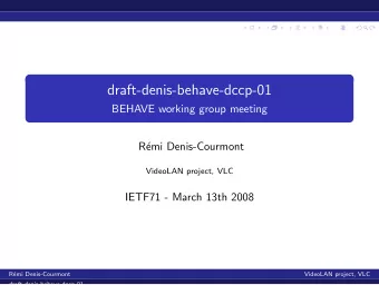
Understanding Radiated EMI Applications Engineering Group MCU - PowerPoint PPT Presentation
Understanding Radiated EMI Applications Engineering Group MCU Division Agenda EMI background Mechanisms Circuit-level causes Frequencies Measurements Shielding Example problem 2 What is Radiated EMI? A digital
Understanding Radiated EMI Applications Engineering Group MCU Division
Agenda ♦ EMI background � Mechanisms � Circuit-level causes � Frequencies � Measurements � Shielding ♦ Example problem 2
What is Radiated EMI? ♦ A digital design can become an unintentional transmitter ♦ Circuit elements can act as antennas � PCB traces � Cables and connections � IC's and devices ♦ This unintentional transmitter can cause problems for other intentional radio systems 108 - 136 MHz 1910 - 1990 MHz 3
Types of Radiated EMI Issues ♦ Regulatory: Fails a spec limit � Examples � System clock harmonics violate EN55022 maximum limits � PWM signal harmonics in an automotive display exceed maximum level allowed by auto maker ♦ Functional: Interferes with itself � Examples � Radio scanner: System clock frequency may jam the receiver � GPS blocking: 16th harmonic of system clock may block GPS reception 4
Agenda ♦ EMI background � Mechanisms � Circuit-level causes � Frequencies � Measurements � Shielding ♦ Example problem 5
Radiation Mechanism: Antennas ♦ Intentional antennas—designed to radiate ♦ Unintentional antennas—not designed to radiate (but do!) 6
Reducing EMI ♦ To eliminate EMI, the engineer must � Reduce the currents or voltages exciting the antennas � Eliminate the transmitting antennas � Block the radiated fields ♦ In practical terms, this is done by � Understanding and minimizing high-frequency sources � Clean PCB layout � Using shielding 7
Agenda ♦ EMI background � Mechanisms � Circuit-level causes � Frequencies � Measurements � Shielding ♦ Example problem 8
What is the Source of EMI? ♦ CMOS digital devices are made of thousands of gates ♦ For simplicity, consider each gate as a CMOS inverter: Vdd Vdd 0 0 9
V DD Current ♦ In dynamic operation, transitions consume current � i CB : Crowbar current � Both gates are momentarily on at the same time, conducting current from Vdd to ground � i L : Load current � Output of the gate is likely connected to input of another gate � Gate inputs are capacitive Vdd Vdd i i i CB i L i CB i L 10
V DD current ♦ Periodic signals through gates cause current impulses Vdd i ♦ Average current depends on switching frequency ♦ Spectrum depends on switching frequency � Usually system clock � Sometimes a subharmonic (sysclk/2, 3, 4, etc) � Peripherals often use sysclk/2 11
V DD Current: DC and AC Components ♦ Think in terms of both AC and DC power supplies � Where does the AC current come from? ♦ Ideal case � Most AC current comes from on-chip sources � Little or no AC current comes from off-chip sources � Small current loop, small antenna 12
V DD Current: DC and AC Components ♦ Realistic case: � AC current is sourced from outside the IC � On-chip capacitors are impractical: silicon area = larger die � Some on-chip capacitance does exist, but not enough ♦ Engineer must think AC currents when designing PCB 13
Think Loop Area ♦ Since AC currents need to flow outside the IC, there will be currents in loops ♦ Current loops = EMI transmitting antennas ♦ Make transmitting loop antennas small ! ♦ Design a short path for the currents � Source currents (from V DD ) � Return currents (through ground) ♦ Silicon Labs MCUs designed with adjacent power and ground pins to minimize loop area 14
Choosing Capacitors ♦ Ideal capacitor (Z C → 0 as frequency → ∞ ) 1 = Z C ω j C ♦ Mag[Z] of an ideal 0.1 uF capacitor: PORT P=1 Z=50 Ohm Capacitor Impedance 100 CAP 10 ID=C1 C=1e5 pF 1 |Z(1,1)| Real Capacitor .1 |Z(1,1)| Ideal Capacitor .01 .001 .0001 .0001 .001 .01 .1 1 10 Frequency (GHz) 15
Choosing Capacitors ♦ Unfortunately there are no ideal capacitors ♦ Real capacitor: capacitor in series with parasitic inductor ♦ Inductor adds impedance with increasing frequency 1 = + ω Z C j L ω j C PORT Parasitic inductance P=1 100 Z=50 Ohm 1 IND ID=L1 L=0.61 nH |Z(1,1)| parasitic inductor .01 CAP ID=C1 C=1e5 pF .0001 .0001 .001 .01 .1 1 10 Frequency (GHz) 16
Choosing Capacitors ♦ Real capacitor—inductance cancels, dominates impedance − j = + ω Z C j L ω Capacitor Impedance C 100 PORT P=1 10 Z=50 Ohm 1 |Z(1,1)| IND Real Capacitor ID=L1 .1 |Z(1,1)| L=0.61 nH Ideal Capacitor .01 0.1uF .001 SRF = 20MHz CAP ID=C1 C=1e5 pF .0001 .0001 .001 .01 .1 1 10 Frequency (GHz) ♦ A capacitor behaves differently in three frequency bands 1. f < SRF: Capacitor acts like a capacitor (Z ↓ as f ↑ ) 2. f = SRF: Reactive impedances cancel 3. f > SRF: Capacitor behaves like an inductor (Z ↑ as f ↑ ) 17
Choosing Capacitors ♦ Wrong capacitor may have little or no effect � Capacitors are capacitors only below SRF � Capacitors are inductors above SRF � Increasing inductive impedance will prevent capacitor from sourcing impulse currents IC PCB Vdd 18
Choosing Capacitors ♦ Solution: select another capacitor � Different capacitor values have different parasitics � Choose capacitor for frequency of interest ♦ Help available from capacitor manufacturers � Murata tool: http://www.murata.com/designlib/mcsil/index.html 19
Capacitor Selection Examples ♦ Compare the imaginary impedance for various Murata capacitors Im[Z] for various Murata caps 40 � 10pF Im(Z(1,1)) 10pF 30 Im(Z(2,2)) 33pF Im(Z(3,3)) (GRM1555C1H100JZ01) 100pF 20 Im(Z(4,4)) 1000pF Im(Z(5,5)) � 33pF 10 1uF 0 (GRM1885C1H330JA01) -10 � 100pF -20 (GRM1555C1H101JZ01) -30 � 1000pF -40 0.03 .1 1 3 (GRM1555C1H102JA01 Frequency (GHz) � 1uF (GRM188F51C105ZA01) 20
Which Capacitor is Best? ♦ Use multiple capacitors in parallel � Example: 10pF || 1000pF || 1uF parallel caps 40 |Z(1,1)| parallel_caps 30 Im(Z(1,1)) parallel_caps 20 10 0 -10 -20 -30 -40 0.03 .1 1 3 Frequency (GHz) 21
Another Reason to Keep Short Traces ♦ Connecting trace to capacitor adds series inductance � Simulate a 3mm trace with via to ground: � Trace is inductive Connecting trace impedance 60 Im(Z(1,1)) EM Structure 1 |Z(1,1)| 40 EM Structure 1 20 0 -20 -40 -60 0.03 .1 1 3 Frequency (GHz) 22
Parallel Caps in Series w ith Trace ♦ Parallel capacitor combination effectiveness is reduced by additional trace inductance parallel caps 40 |Z(1,1)| parallel_caps 30 Im(Z(1,1)) parallel_caps 20 10 0 -10 -20 -30 -40 0.03 .1 1 3 Frequency (GHz) 23
Internal Coupling/Leakage ♦ EMI can result from AC energy coupling to digital I/O lines inside the IC ♦ Static digital I/O's may be a source of EMI ♦ Possible causes: � Conduction through power supply � Capacitive coupling � Inductive coupling IC PCB Vdd 24
Internal Coupling/Leakage ♦ Consider a simplified model � Think of the EMI as a noise source with some impedance coupling it to a digital I/O � Current at the digital I/O is from two sources � Digital driver (good) � EMI (bad) IC PCB Vdd Vnoise 25
Internal Coupling/Leakage ♦ How should we block the noise? Add a capacitor? ♦ May make EMI worse � Capacitor provides a low-impedance path outside the IC � The low impedance path may increase current IC PCB Vdd Vnoise 26
Internal Coupling/Leakage ♦ Add series resistance? May help � Less current (good and bad current) flows through high impedance � May reduce EMI by reducing currents flowing outside IC IC PCB Vdd Vnoise ♦ Disadvantage � Adding resistance may attenuate or distort the wanted signal For example, it may not provide enough LED current, or may slow a signal's slew rate 27
Internal Coupling/Leakage ♦ Troubleshooting experiment � Set R = ∞ by lifting pin � Reduced EMI means that this pin is contributing IC PCB Vdd Vnoise 28
Internal Coupling/Leakage ♦ Add an external inductor or choke? � Provides high impedance for high frequencies, low impedance for low frequencies IC PCB Vdd Vnoise ♦ Disadvantages � Inductor may actually create and radiate EMI (inductors turn electric currents into magnetic fields) � Inductors cost more than resistors and capacitors 29
Agenda ♦ EMI background � Mechanisms � Circuit-level causes � Frequencies � Measurements � Shielding ♦ Example problem 30
Time and Frequency Domains ♦ Signals can be represented in time or frequency domains � Fourier transform F : Transform between time and frequency domains � Digital designers think in time domain � EMI measurements are in the frequency domain ♦ Periodic events in a circuit create distinct EMI frequencies � Frequencies often harmonics of the system clock � Frequencies may be harmonics of system clock subharmonics � Example: Flash memory read every third sysclock period � Digital waveforms will create harmonics � Square wave creates odd harmonics � Impulse train creates even and odd harmonics 31
Fourier Transform Review ♦ Square wave � Square wave is composed of several odd harmonics 32
Fourier Transform Review ♦ Impulse train � A series of pulses in time is a series of tones in frequency 33
Recommend
More recommend
Explore More Topics
Stay informed with curated content and fresh updates.
