Tracking and Timing with Induced Current Detectors Ronald Lipton - PowerPoint PPT Presentation
Tracking and Timing with Induced Current Detectors Ronald Lipton CPAD 2019 Dec. 10 2019 Introduction There has been increasing interest in fast timing as well as intelligent detector systems. I would like to present some ideas for
Tracking and Timing with Induced Current Detectors Ronald Lipton CPAD 2019 Dec. 10 2019
Introduction There has been increasing interest in fast timing as well as “intelligent” detector systems. I would like to present some ideas for alternate designs of such systems looking at how technology for silicon-based detectors might evolve. This is a talk about the future - next generation of collider experiments. We focus on capability enabled by new technologies that provide small pixels with low capacitance and sophisticated processing • 3D integration of sensors and electronics • Monolithic active devices • Semiconductor substrate engineering 12/10/2019 Ronald Lipton 2
Some Basics - time resolution • The rule of thumb for the time resolution of a system dominated by jitter is: Jitter Front end noise Time resolution 2 + t d ( ) 2 4 ktA ⎛ ⎞ 2 ∂ V ⎛ ⎞ t a C L Noise 2 = C L σ t ~ σ t ~ σ noise σ n ⎜ ⎟ ~ t r ⎜ ⎟ ⎝ ⎠ ∂ t ⎝ ⎠ Signal g m t a Signal g m t a • slew rate (dV/dt) is related to the inverse amplifier rise time, C L is the load capacitance t d and t a are the detector and amplifier rise times and g m is the input transistor transductance - related to input current, and A is a characteristic of the amplifier. • Fast timing -> large S/N, fast amp, small load capacitance • There are tradeoffs available 12/10/2019 Ronald Lipton 3
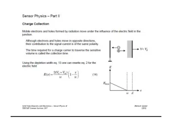
More Basics - Signal Development • Signal induced by moving charges ! E w × ! depends on work done by circuit. The i = − q v charge induced on an electrode depends ! d ! on the coupling between the moving ∫ ∫ Q s = idt = q E w x charge and the electrode (Ramo’s theorem) Q 1 → 2 = q ( V w 2 − V w 1 ) • We usually work with simple parallel plate systems • In a multi-electrode system the induced current on an electrode depends on the velocity of the charge and the value of the effective “weighting” field • Weighting field is calculated with 1 V on measuring elected, 0 V on others • There are fast transient induced currents on neighbor electrodes that integrate to zero - can we use them? 12/10/2019 Ronald Lipton 4
3D Integration and small pixels Fermilab has been involved the development of 3D sensor/ASIC integration for almost a decade and have demonstrated (with industrial partners): • Hybrid bonding technology • .5 mm Oxide bonding with imbedded metal sensor through silicon vias (TSV) (BNL) • Bond pitch of 4 microns 34 micron • high 2-tier First 3-tier electronics-sensor stack VICTR chip • Small pixels with ADC, TDC (24 microns) 500" • Small TSV capacitance (~7 ff) 450" Unbonded" 400" The noise in hybrid bonded VIPIC 3D • Bump"bonded" 350" Fusion"Bonded" assembly is almost a factor of two lower 300" Counts' 250" than the equivalent conventionally bump 200" 150" bonded parts due to lower C load 100" 50" 0" 25" 30" 35" 40" 45" 50" 55" 60" 65" 12/10/2019 Ronald Lipton 5 noise'(electrons)'
3D 9 pixel model Methodology We explore simple systems with various pixel sizes, detector thickness and pulse shapes • Build a (Silvaco) TCAD (2D or 3D) detector model • Inject a Q tot =4 fc pulse • Extract the capacitance and pulse shapes at the electrodes • Inject the resulting pulse into a SPICE model Pulses from “x-ray” at~100 μ 200 μ thick detector of a generic 65nm charge sensitive amplifier including noise TCAD Simulation • Analyze the characteristics of the 3 E-14 200 Micron Thick Detector Capacitance (farads) 2 .5E-14 Farads/micron resulting output pulses 2 E-14 • For angled track studies I use simple op amp 1 .5E-14 with defined bandwidth model with adjustable 1 E-14 5 E-15 bandwidth y = 2E-18x 2 + 1E-16x + 1E-15 0 0 20 40 60 80 100 120 Pixel Pitch (microns) 12/10/2019 Ronald Lipton 6
Simple Example - X-Rays Suppose an application requires fast timing on high energy x-rays • Usually we would like thin detectors for fast timing, but thin detectors imply low efficiency - can we use induced currents to achieve time resolution in a thick detector? Central pixel Initial Current Spike Edge neighbor (diffusion collected charge) Corner neighbor 0 collected charge 12/10/2019 Ronald Lipton 7
Pulse Shapes - 200 micron detector Χ -ray 2D Simulation Central Electrode z=10 z=10 z=100 z=190 2ns 2ns z=100 z=190 Central = n n+1 n+2 n+3 2ns 12/10/2019 2ns Ronald Lipton 8
X-Ray With Noise at 185/200 micron depth • Apply a constant threshold of E1~10 mV, E4~130 mV • Tabulate time at threshold crossing including noise • Edge pixel can provide a “start” time stamp if needed Edge pixel E1 Edge pixel σ ~ 30ps 730 mV 720 mV 10 ns Timing histogram Central pixel h h 10 25 25 Entries Entries 104.5 104.5 Mean Mean Central pixel 0.0204 0.0204 Std Dev Std Dev χ χ 2 2 / ndf / ndf 0.4421 / 2 0.4421 / 2 Constant Constant 9.179 9.179 ± ± 2.457 2.457 Mean Mean 104.5 104.5 ± ± 0.0 0.0 Sigma Sigma 0.02177 0.02177 0.00445 0.00445 ± ± 8 σ ~ 22ps 6 850 mV 4 2 12/10/2019 Ronald Lipton 9 0 104 104.2 104.4 104.6 104.8 105
Example - MIP in a 50 micron Detector σ ~25 micron pitch, 50 microns thick 200 Pulse on central pixel V, sensor potential distribution 2ns Amplifier output with noise, 20ff load Timing histogram h h Entries Entries 26 26 Mean Mean 102.3 102.3 12 Std Dev Std Dev 0.01593 0.01593 c c 2 2 / ndf / ndf 0.6285 / 1 0.6285 / 1 ± ± Constant Constant 12.34 12.34 3.24 3.24 ± ± Mean Mean 102.3 102.3 0.0 0.0 ± ± Sigma Sigma 0.01657 0.01657 0.00311 0.00311 10 σ ~16ps 8 Threshold 6 4 2 12/10/2019 Ronald Lipton 10 0 102 102.1 102.2 102.3 102.4 102.5 102.6 102.7
Comments The 20-30 ps resolution will be degraded in a real system However: • All pixels with spacing small compared to depth will have similar signals ~ 16 pixels for a 25x200 micron sensor x 4 in (uncorrelated) time resolution • The central pixel will see a large signal within a few ns of the leading edge - initial thresholds can be set low and signals latched only if a central pixel fires at a higher threshold • The pattern of pixels will provide depth and slope information • Multiple thresholds or more sophisticated processing can give a time walk correction • These results are for n-on-p with maximum field at the top. n-on-n sensors have a maximum field at the bottom. The field profiles can be adjusted to suit the application by varying the applied bias 12/10/2019 Ronald Lipton 11
CMS “P t module” Pattern Recognition Collider based experiments have to deal with increasingly complex events • HL LHC with ~200 interactions per crossing • The CMS experiment is addressing this with stacked sensor arrays to distinguish low from moderate momentum tracks • Can we do this in a single sensor? • Muon collider experiments with huge decay backgrounds • Muon collider studies use timing - fall x 100 short • Backgrounds are from various absorber surfaces/angles • We can use the pattern of electrode signals to distinguish between signal and background tracks signatures To get a feeling for this we use a 25 micron pitch electrode geometry in a ~300 micron thick sensor. 12/10/2019 Ronald Lipton 12
Charge Motion Visualization 30 degree track, n on n, maximum field at bottom. electrons holes .1 ns .5 ns 1.0 ns 1.5 ns 2 ns 2.5 ns 12/10/2019 Ronald Lipton 13
MIPs at various angles Current (Arb. Units) Current (Arb. Units) 0 Deg 10 Deg 10ns 10ns Transient time. Transient time. Current (Arb. Units) Current (Arb. Units) 20 Deg 30 Deg 10ns 10ns 12/10/2019 Ronald Lipton 14
Time resolution and Pattern Recognition 1.40E-05 E4 E4 E2 E6 1.20E-05 1ns Iin 1.00E-05 2ns • 8.00E-06 6.00E-06 4.00E-06 2.00E-06 0.00E+00 0.00E+00 2.00E-09 4.00E-09 6.00E-09 8.00E-09 1.00E-08 1.20E-08 1.40E-08 Long drift 2.00E-06 • some collected charge Electrode 6 1.80E-06 • dominated by induced current Iin 1.60E-06 • difficult to measure secondary peak 2ns 1.40E-06 Medium drift 1ns 1.20E-06 • Dominated by collected charge 1.00E-06 Short drift 8.00E-07 • collected charge similar to induced current 6.00E-07 • Induced and collected 4.00E-07 signals merge 2.00E-07 0.00E+00 0.00E+00 2.00E-09 4.00E-09 6.00E-09 8.00E-09 1.00E-08 1.20E-08 1.40E-08 12/10/2019 Ronald Lipton 15
A look at angular resolution 6.00E-06 10 Degree Track E2 5.00E-06 • To try to get a feeling for what time and pulse E3 E4 height resolution is needed we look at 10 and 20 4.00E-06 E5 degree tracks E6 Signal (Arb Units) 3.00E-06 • 1 nanosecond rise time is assumed 2.00E-06 • Lowest threshold defines time resolution and provides induced 1.00E-06 current t0 0.00E+00 • Other thresholds provide time structure and shape -1.00E-06 of secondary peak 0.00E+00 5.00E-09 1.00E-08 1.50E-08 2.00E-08 Time (Sec) 6.00E-06 1.00E-06 20 Deg Track 20 Degree Track E2 E2 5.00E-06 E3 E3 E4 8.00E-07 E4 E5 E5 4.00E-06 E6 E6 6.00E-07 Sig (Arb Units) 3.00E-06 Sig (Arb Units) 2.00E-06 4.00E-07 ToT end Threshold 1.00E-06 2.00E-07 0.00E+00 ToT start Threshold -1.00E-06 0.00E+00 0.00E+00 5.00E-09 1.00E-08 1.50E-08 2.00E-08 0.00E+00 5.00E-09 1.00E-08 1.50E-08 2.00E-08 Time (sec) Time (sec) 12/10/2019 Ronald Lipton 16
Recommend
More recommend
Explore More Topics
Stay informed with curated content and fresh updates.
